
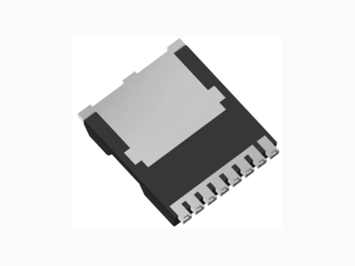
PDT49I0B POTENS
Document overview
- Manufacturer or author: Provided By www.digicamel.com(free datasheet download site)
- PDF pages: 6
Technical content
Features
Absolute Maximum Ratings Tc=25℃ unless otherwise noted Thermal Characteristics Applications TOLL Pin Configuration D G S G Motor Driver Load Switch Power Tools D S S S S S S S S S S S S S S G D
Potens semiconductor corp. Ver.1.00 PDT49I0B 40V N-Channel MOSFETs Off Characteristics Symbol Parameter Conditions Min. Typ. Max. Unit BVDSS Drain-Source Breakdown Voltage VGS=0V , ID=250µA 40 --- --- V IDSS Drain-Source Leakage Current VDS=40V , VGS=0V , TJ=25℃ --- --- 1 µA VDS=32V , VGS=0V , TJ=85℃ --- --- 10 µA IGSS Gate-Source Leakage Current VGS=±20V , VDS=0V --- --- ±100 nA On Characteristics RDS(ON) Static Drain-Source On-Resistance VGS=10V , ID=20A --- 0.55 0.65 m VGS=4.5V , ID=10A --- 0.77 1 m VGS(th) Gate Threshold Voltage VGS=VDS , ID =250µA 1.2 1.6 2.5 V Dynamic and switching Characteristics3 Qg Total Gate Charge VDS=20V , VGS=10V , ID=80A --- 210 315 nC VDS=20V , VGS=4.5V , ID=80A --- 110 165 Qgs Gate-Source Charge --- 19 30 Qgd Gate-Drain Charge --- 50 75 Td(on) Turn-On Delay Time VDD=20V , VGS=10V , RG=6 ID=80A --- 30 45 ns Tr Rise Time --- 40 60 Td(off) Turn-Off Delay Time --- 80 120 Tf Fall Time --- 110 165 Ciss Input Capacitance VDS=20V , VGS=0V , F=1MHz --- 9750 15000 pF Coss Output Capacitance --- 3700 5600 Crss Reverse Transfer Capacitance --- 500 750 Rg Gate resistance VGS=0V, VDS=0V, F=1MHz --- 1 --- Symbol Parameter Conditions Min. Typ. Max. Unit EAS Single Pulse Avalanche Energy VDD=25V, L=0.1mH, IAS=100A 500 --- --- mJ Symbol Parameter Conditions Min. Typ. Max. Unit IS Continuous Source Current VG=VD=0V , Force Current --- --- 300 A ISM Pulsed Source Current --- --- 600 A VSD Diode Forward Voltage VGS=0V , IS=1A , TJ=25℃ --- --- 1 V trr Reverse Recovery Time VR=30V, IS=10A di/dt=100A/µs, TJ=25℃ --- 210 --- ns Qrr Reverse Recovery Charge --- 750 --- nC Note : 1. Repetitive Rating : Pulsed width limited by maximum junction temperature. 3. Essentially independent of operating temperature. Electrical Characteristics (TJ=25 ℃, unless otherwise noted) Drain-Source Diode Characteristics and Maximum Ratings Guaranteed Avalanche Energy
Potens semiconductor corp. Ver.1.00 PDT49I0B 40V N-Channel MOSFETs 120 150 180 0 1 2 3 4 5 VGS=2.7V VGS=3V VGS=4.5V VGS=3.5V VGS=3.3V 0.4 0.6 0.8 1.2 1.4 -50 0 50 100 150 120 180 240 300 25 50 75 100 125 150 0 2 4 6 8 10 Tc=25℃ ID=20A 0.0 0.2 0.4 0.6 0.8 1.0 5 45 85 125 165 205 Tc=25℃ VGS=4.5V VGS=10V 0.5 1.5 2.5 -50 0 50 100 150 ID , Continuous Drain Current (A) Fig.1 Typical Output Characteristics ID , Continuous Drain Current (A) TC , Case Temperature (℃) Fig.2 Continuous Drain Current vs. TC Normalized On Resistance TJ , Junction Temperature (℃) Fig.3 Normalized RDSON vs. TJ Normalized Gate Threshold V oltage TJ , Junction Temperature (℃) Fig.4 Normalized Vth vs. TJ RDS(ON) , Turn-On Resistance (mohm) Fig.5 Turn-On Resistance vs. VGS Fig.6 Turn-On Resistance vs. ID RDS(ON) , Turn-On Resistance (mohm) VDS ,Drain to Source V oltage (V) VGS , Gate to Source V oltage (V) ID , Drain Current (A)
Potens semiconductor corp. Ver.1.00 PDT49I0B 40V N-Channel MOSFETs Fig.10 Maximum Safe Operation Area Fig.11 Switching Time Waveform Fig.12 Gate Charge Waveform Fig.8 Gate Charge Characteristics VGS 10V / 4.5V Qg QgdQgs Gate Charge Td(on) Tr Ton Td(off) Tf Toff VDS VGS 90% 10% 0.01 0.1 NOTES: DUTY FACTOR: D = t1/t2SINGLE PULSE 0.5 0.2 0.1 0.05 0.02 0.01 0 30 60 90 120 150 180 ID=80A VDS=20V 100 1000 10000 0.1 1 10 Ciss Coss Crss 0.1 100 1000 0.1 1 10 100 TC=25℃ DC 100ms 10ms 100µs 10µs 1ms VDS , Drain to Source V oltage (V) Qg , Gate Charge (nC) Normalized Thermal Response VGS , Gate to Source V oltage (V) (mohm) Fig.9 Normalized Transient Impedance Square Wave Pulse Duration (s) VDS , Drain to Source V oltage (V) ID , Continuous Drain Current (A) Capacitance (pF) Fig.7 Capacitance Characteristics
Potens semiconductor corp. Ver.1.00 PDT49I0B 40V N-Channel MOSFETs SYMBOL mm SYMBOL mm MIN NOM MAX MIN NOM MAX A1 1.70 1.80 1.90 H1 6.95 BSC b 0.70 0.80 0.90 H2 5.89 BSC b1 9.70 9.80 9.90 i 0.10 REF b3 1.10 1.20 1.30 j 0.46 REF c 0.40 0.50 0.60 K 2.80 REF E 9.80 9.90 10.00 N 8 E1 8.00 8.10 8.20 Q 8.00 REF e 1.20 BSC θ 10o REF TOLL PACKAGE INFORMATION
Potens semiconductor corp. Ver.1.00 PDT49I0B 40V N-Channel MOSFETs TOLL RECOMMENDED LAND PATTERN unit : mm