
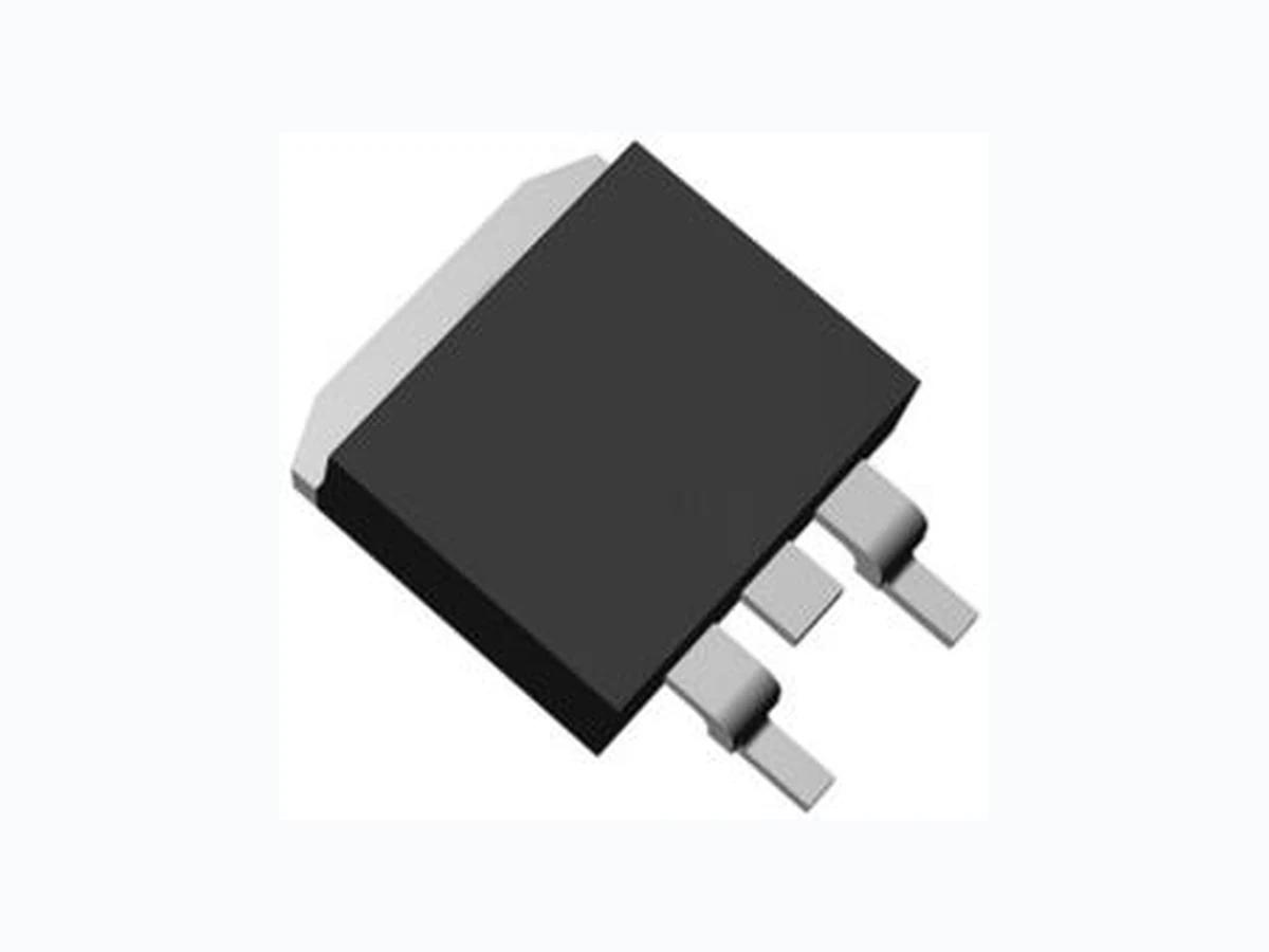
PDH0959 POTENS
Document overview
- Manufacturer or author: Provided By www.digicamel.com(FREE DATASHEET DOWNLOAD SITE)
- PDF pages: 6
Technical content
Features
Absolute Maximum Ratings (Tc=25℃ unless otherwise noted) Thermal Characteristics D G S Networking Load Switch LED applications D S G
Potens semiconductor corp. Ver.1.01 PDH0959 100V P-Channel MOSFETs Off Characteristics Symbol Parameter Conditions Min. Typ. Max. Unit BVDSS Drain-Source Breakdown Voltage VGS=0V , ID=-250µA -100 --- --- V IDSS Drain-Source Leakage Current VDS=-100V , VGS=0V , TJ=25℃ --- --- -1 µA VDS=-80V , VGS=0V , TJ=85℃ --- --- -10 µA IGSS Gate-Source Leakage Current VGS=±20V , VDS=0V --- --- ±100 nA On Characteristics RDS(ON) Static Drain-Source On-Resistance VGS=-10V , ID=-15A --- 32 38 m VGS=-4.5V , ID=-10A --- 36 47 m VGS(th) Gate Threshold Voltage VGS=VDS , ID =-250µA -1.2 -1.6 -2.5 V Dynamic and switching Characteristics Qg Total Gate Charge3,4 VDS=-50V , VGS=-10V , ID=-20A --- 92 140 nC Qgs Gate-Source Charge3,4 --- 13 20 Qgd Gate-Drain Charge3,4 --- 14 20 Td(on) Turn-On Delay Time3,4 VDD=-50V , VGS=-10V , RG=6 ID=-20A --- 10 15 ns Tr Rise Time3,4 --- 15 25 Td(off) Turn-Off Delay Time3,4 --- 20 30 Tf Fall Time3,4 --- 25 40 Ciss Input Capacitance VDS=-50V , VGS=0V , F=1MHz --- 5700 8550 pF Coss Output Capacitance --- 160 240 Crss Reverse Transfer Capacitance --- 120 180 Symbol Parameter Conditions Min. Typ. Max. Unit EAS Single Pulse Avalanche Energy VDD=50V, L=0.1mH, IAS=46A 105.8 --- --- mJ Symbol Parameter Conditions Min. Typ. Max. Unit IS Continuous Source Current VG=VD=0V , Force Current --- --- -35 A ISM Pulsed Source Current --- --- -70 A VSD Diode Forward Voltage VGS=0V , IS=-1A , TJ=25℃ --- --- -1 V trr Reverse Recovery Time VR=-50V, IS=-10A di/dt=100A/µs, TJ=25℃ --- 55 --- ns Qrr Reverse Recovery Charge --- 60 --- nC Note : 1. Repetitive Rating : Pulsed width limited by maximum junction temperature. 2. VDD=-50V,VGS=-10V,L=0.1mH,IAS=-60A.,Starting TJ=25℃ 3. The data tested by pulsed , pulse width ≦ 300µs , duty cycle ≦ 2%. 4. Essentially independent of operating temperature. Electrical Characteristics (TJ=25 ℃, unless otherwise noted) Drain-Source Diode Characteristics and Maximum Ratings Guaranteed Avalanche Energy
Potens semiconductor corp. Ver.1.01 PDH0959 100V P-Channel MOSFETs 0.4 0.6 0.8 1.2 1.4 -50 0 50 100 150 0.5 1.5 2.5 -50 0 50 100 150 25 50 75 100 125 150 0 2 4 6 8 10 VGS=-4.5V VGS=-3V VGS=-3.3V VGS=-3.5V 2 4 6 8 10 Tc=25℃ ID=-10A ID=-15A 5 10 15 20 25 30 Tc=25℃ VGS=-4.5V VGS=-6V VGS=-10V -ID , Continuous Drain Current (A) Fig.1 Typical Output Characteristics -ID , Continuous Drain Current (A) TC , Case Temperature (℃) Fig.2 Continuous Drain Current vs. TC Normalized On Resistance TJ , Junction Temperature (℃) Fig.3 Normalized RDSON vs. TJ Normalized Gate Threshold V oltage TJ , Junction Temperature (℃) Fig.4 Normalized Vth vs. TJ RDS(ON) , Turn-On Resistance (mohm) Fig.5 Turn-On Resistance vs. VGS Fig.6 Turn-On Resistance vs. ID RDS(ON) , Turn-On Resistance (mohm) -VDS ,Drain to Source V oltage (V) -VGS , Gate to Source V oltage (V) -ID , Drain Current (A)
Potens semiconductor corp. Ver.1.01 PDH0959 100V P-Channel MOSFETs Fig.10 Maximum Safe Operation Area Fig.11 Switching Time Waveform Fig.12 Gate Charge Waveform Fig.8 Gate Charge Characteristics -VGS -10V / -4.5V Qg QgdQgs Gate Charge Td(on) Tr Ton Td(off) Tf Toff VDS VGS 90% 10% 0.01 0.1 NOTES: DUTY FACTOR: D = t1/t2SINGLE PULSE 0.5 0.2 0.1 0.05 0.02 0.01 100 1000 10000 0.1 1 10 100 Ciss Coss Crss 0 20 40 60 80 100 ID=-20A VDS=-50V 0.01 0.1 100 0.1 1 10 100 TC=25℃ DC 100ms 10ms 100µs 10µs 1ms -VDS , Drain to Source V oltage (V) Qg , Gate Charge (nC) Normalized Thermal Response -VGS , Gate to Source V oltage (V) (mohm) Fig.9 Normalized Transient Impedance Square Wave Pulse Duration (s) -VDS , Drain to Source V oltage (V) -ID , Continuous Drain Current (A) Capacitance (pF) Fig.7 Capacitance Characteristics
Potens semiconductor corp. Ver.1.01 PDH0959 100V P-Channel MOSFETs Symbol Dimensions In Millimeters Dimensions In Inches MAX MIN MAX MIN A 4.850 4.200 0.191 0.165 A1 0.300 0.000 0.012 0.000 A2 2.900 2.200 0.114 0.087 b 0.950 0.700 0.037 0.028 b2 1.700 1.000 0.067 0.039 c 1.450 1.150 0.057 0.045 D 9.500 8.350 0.374 0.329 D1 9.150 6.400 0.360 0.252 E 10.500 9.600 0.413 0.378 E1 8.900 6.850 0.350 0.270 e 2.540 BSC 0.100 BSC H 15.900 14.600 0.626 0.575 L 2.800 1.700 0.110 0.067 L1 1.700 1.050 0.067 0.041 L2 2.100 1.300 0.083 0.051 L3 0.250 BSC 0.010 BSC L4 0.750 0.200 0.030 0.008 TO263 PACKAGE INFORMATION
Potens semiconductor corp. Ver.1.01 PDH0959 100V P-Channel MOSFETs TO263 RECOMMENDED LAND PATTERN unit : mm