
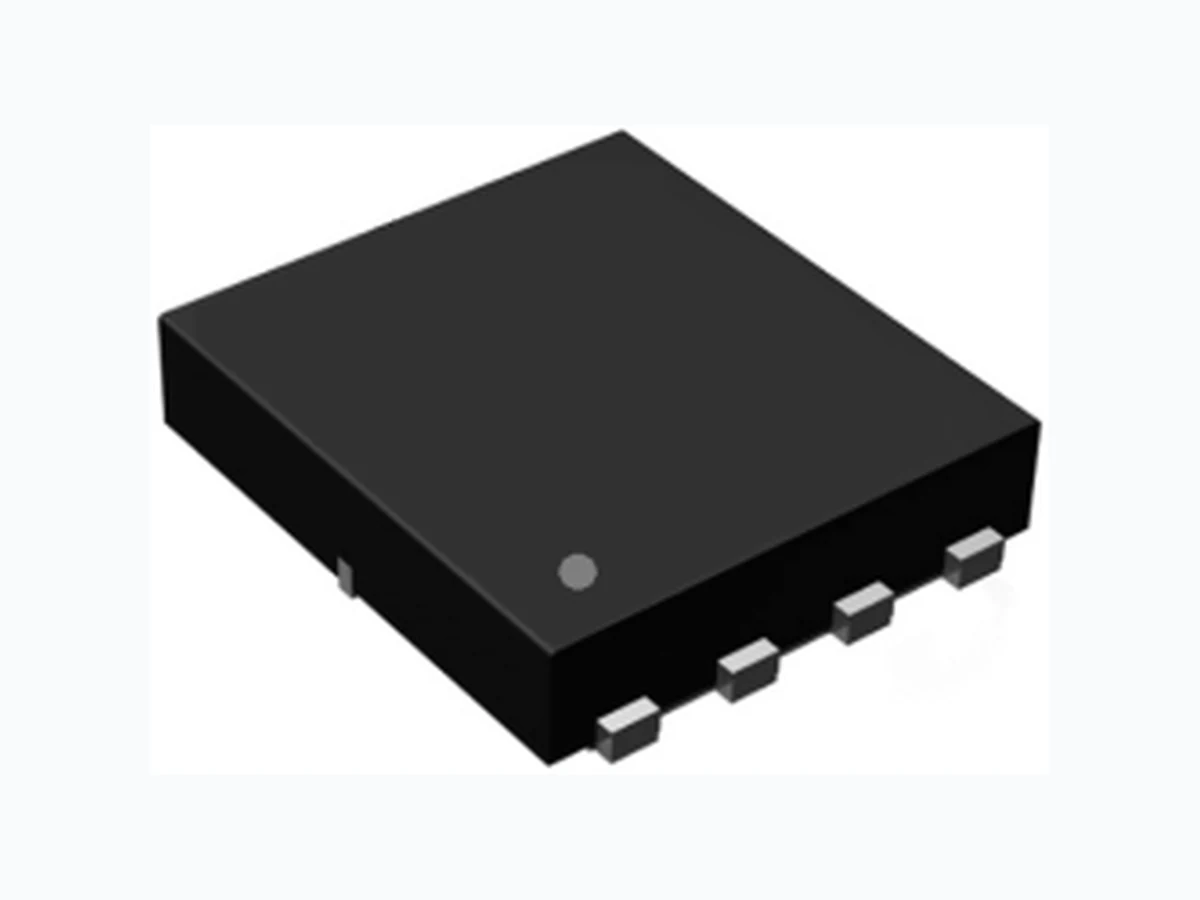
PDC0810T POTENS
Document overview
- Manufacturer or author: Provided By www.digicamel.com(free datasheet download site)
- PDF pages: 6
Technical content
Features
Absolute Maximum Ratings Tc=25℃ unless otherwise noted Thermal Characteristics D1 D1 G1 S1
Applications
Networking Load Switch LED applications PPAK5x6 Dual Pin Configuration G1 G2 D1 D2 S1 S2
Potens semiconductor corp. Ver.1.01 PDC0810T 100V Dual N-Channel MOSFETs Off Characteristics Symbol Parameter Conditions Min. Typ. Max. Unit BVDSS Drain-Source Breakdown Voltage VGS=0V , ID=250uA 100 --- --- V △BVDSS/△TJ BVDSS Temperature Coefficient Reference to 25℃ , ID=1mA --- 0.10 --- V/℃ IDSS Drain-Source Leakage Current VDS=100V , VGS=0V , TJ=25℃ --- --- 1 uA VDS=80V , VGS=0V , TJ=125℃ --- --- 10 uA IGSS Gate-Source Leakage Current VGS=±20V , VDS=0V --- --- ±100 nA RDS(ON) Static Drain-Source On-Resistance2 VGS=10V , ID=4A --- 145 185 m VGS=4.5V , ID=2A --- 150 195 m VGS(th) Gate Threshold Voltage VGS=VDS , ID =250uA 1.2 1.8 2.5 V △VGS(th) VGS(th) Temperature Coefficient --- -4 --- mV/℃ gfs Forward Transconductance VDS=10V , ID=1A --- 5 --- S Qg Total Gate Charge2 , 3 VDS=50V , VGS=10V , ID=2A --- 13.4 21 nC Qgs Gate-Source Charge2 , 3 --- 2.9 6 Qgd Gate-Drain Charge2 , 3 --- 1.7 4 Td(on) Turn-On Delay Time2 , 3 VDD=30V, VGS=10V , RG=3.3 ID=1A --- 1.6 3 ns Tr Rise Time2 , 3 --- 6.6 13 Td(off) Turn-Off Delay Time2 , 3 --- 11.5 22 Tf Fall Time2 , 3 --- 3.6 7 Ciss Input Capacitance VDS=25V , VGS=0V , F=1MHz --- 820 1190 pF Coss Output Capacitance --- 35 55 Crss Reverse Transfer Capacitance --- 20 30 Rg Gate resistance VGS=0V, VDS=0V, F=1MHz --- 1.3 2.6 Symbol Parameter Conditions Min. Typ. Max. Unit IS Continuous Source Current VG=VD=0V , Force Current --- --- 10 A ISM Pulsed Source Current2 --- --- 20 A VSD Diode Forward Voltage2 VGS=0V , IS=1A , TJ=25℃ --- --- 1 V Electrical Characteristics (TJ=25 ℃, unless otherwise noted) Note : 1. Repetitive Rating : Pulsed width limited by maximum junction temperature. 2. The data tested by pulsed , pulse width ≦ 300us , duty cycle ≦ 2%. 3. Essentially independent of operating temperature. Drain-Source Diode Characteristics Dynamic Characteristics On Characteristics
Potens semiconductor corp. Ver.1.01 PDC0810T 100V Dual N-Channel MOSFETs Fig.1 Continuous Drain Current vs. TC Fig.3 Normalized Vth vs. TJ ID , Continuous Drain Current (A) Normalized On Resistance Fig.2 Normalized RDSON vs. TJ Normalized Gate Threshold V oltage VGS , Gate to Source V oltage (V) Fig.4 Gate Charge Waveform Normalized Thermal Response ID , Continuous Drain Current (A) Fig.6 Maximum Safe Operation Area Fig.5 Normalized Transient Impedance TJ , Junction Temperature (℃) Qg , Gate Charge (nC) VDS , Drain to Source V oltage (V) Square Wave Pulse Duration (s) TC , Case Temperature (℃) TJ , Junction Temperature (℃)
Potens semiconductor corp. Ver.1.01 PDC0810T 100V Dual N-Channel MOSFETs Td(on) Tr Ton Td(off) Tf Toff VDS VGS 90% 10% IAS VGS BVDSS VDD EAS= 1
2 L x IAS
Fig.8 EAS Waveform Fig.7 Switching Time Waveform
Potens semiconductor corp. Ver.1.01 PDC0810T 100V Dual N-Channel MOSFETs Symbol Dimensions In Millimeters Dimensions In Inches Min Max Min Max A 0.800 1.200 0.031 0.047 b 0.300 0.510 0.012 0.020 C 0.250 Ref 0.010 Ref D 4.800 5.400 0.189 0.213 E 5.450 5.960 0.215 0.235 E1 3.200 3.800 0.126 0.150 e 1.27 BSC 0.050 BSC F 1.000 1.900 0.039 0.075 G 0.380 0.800 0.015 0.031 H 5.850 6.300 0.230 0.248 L1 0.050 0.250 0.002 0.010 K 1.500 1.900 0.059 0.074 PPAK5x6 Dual PACKAGE INFORMATION
Potens semiconductor corp. Ver.1.01 PDC0810T 100V Dual N-Channel MOSFETs PPAK5X6 Dual RECOMMENDED LAND PATTERN unit : mm