
DATASHEET SEARCH SITE
Document overview
- Manufacturer or author: Provided By www.digicamel.com(FREE DATASHEET DOWNLOAD SITE)
- PDF pages: 16
Technical content
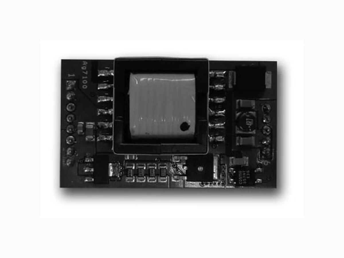
V1.0 May 2015 Datasheet Ag7100 57V Boost Converter Module © Silver Telecom 2015 1 Silvertel 1. Features ¾ Small package ¾ Suitable for IEEE802.3af and IEEE802.3at compliant PSEs ¾ Low cost ¾ High efficiency (>90%) ¾ Input voltage range 12V to 27V ¾ Minimal external components required ¾ Short-circuit and Thermal protection ¾ Adjustable Output (48V to 57V) ¾ 1500V isolation (input to output) ¾ Silvertel “design-in” assistance 2. Description The Ag7100 module is a low noise DC/DC boost converter, designed to generate the higher voltages required for IEEE802.3 PSE applications from lower voltage supplies. This module provides exceptional efficiency (>90%) while providing full compatibility with the IEEE 802.3af and 802.3at power and isolation requirements. The module accepts a wide DC voltage input range, from 12V to 27V. The input voltage is then boosted to generate the higher voltages required to power Silvertel’s PSE modules (or compatible PSE circuits). The Ag7100 pr ovides a regulated adjustable output, of between 48V and 57V. This provides com patibility with both IE EE802.3af and the higher power POE+ 802.3at PSE standards. Ag7100 has been designed to provide an ideal solu tion for powering the Silvertel Ag6100 PSE module from a vehicle battery, 12V plug -top PSU or other commonly available power supplies. Its low cost, small footprint, high e fficiency and in-built isolation make it an extremely versatile DC-DC boost converter for a wide range of potential applications. PbPb
V1.0 May 2015 Ag7100 Data Sheet 57V Boost Converter Module © Silver Telecom 2015 3 3. Ag7100 Product Selector Part Number† Output Voltage Maximum Output Power * Date code‡ and Voltage Marking Ag7100 48V to 57V 40 Watts WWYY A *At 25°C with V IN = 24V † The Ag7100 fully meets the requirements of the RoHS directive 2011/65/EC on the restriction of hazardous substances in electronic equipment. ‡ Date code format: “WW” = Week Number, “YY” = Year. Table 1: Ordering Information Figure 1: Block Diagram
V1.0 May 2015 Ag7100 Data Sheet 57V Boost Converter Module © Silver Telecom 2015 4 4. Pin Description Figure 2: Ag7100 Package Format
V1.0 May 2015 Ag7100 Data Sheet 57V Boost Converter Module © Silver Telecom 2015 5
4.1 Ag7100
Pin # Name Description VIN+ Direct Input +. These pins connect to the positive (+) output of the power supply. 2 IC Internal Connection. Do not connect to these pins. VIN- Direct Input -. These pins connect to the negative (-) output of the power supply. 8 +VDC DC Output. These pins provides the regulated output from the DC/DC converter. 10
11 ADJ
Output Adjust. The output voltage can be adjusted down from its nominal value of 57V. This can be done by connecting an external resistor from this pin to the +VDC pins. -VDC DC Return. These pin are the return path for the +VDC output. Table 2: Pin Description
V1.0 May 2015 Ag7100 Data Sheet 57V Boost Converter Module © Silver Telecom 2015 6 5. Functional Description
5.1 Input
The Ag7100 has a wide input voltage range of 12Vdc to 27Vdc; as shown in Figure 3. The 470µF 36V electrolytic connected across the Ag7100 input, is r equired to reduce the ripple from the supply. This value can be adjusted, depending on the quality of the power supply being used. Figure 3: Typical System Diagram
5.2 Output
The Ag7100 output must have an external 47µF 63V electrolyt ic capacitor fitted. This capacitor must be fitted as close as possible to the output pins. It functions as part of the output filter and is required to reduce the DC/DC converter switching noise and output ripple. To reduce the output ripple and noise furt her, we would recommend using a low ESR electrolytic. Also a low ESR capacitor is essential for operation below 0°C.
V1.0 May 2015 Ag7100 Data Sheet 57V Boost Converter Module © Silver Telecom 2015 7
5.3 Isolation
To meet the safety isolation requirements of Power over Ethernet (PoE); the Ag7100 has been designed to meet the 1500Vdc impulse test*. It is also important that the tracks on either side of the isolation ba rrier also have at least a 3mm clearance, see Figure 6 in Section 6 for more information. *Note: The impulse test is defined in the following specifications: - IEEE802.3af section 33.4.1 option b IEEE802.3at section 33.4.1 option c
5.4 DC/DC Converter
The Ag7100 DC/DC converter provides a r egulated output that has built-in over temperature and output short-circuit protection.
5.5 Output Adjustment
The Ag7100 has a nominal out put voltage of 57V. This can be adjusted down to a minimum of 48V, by fitting a resistor between the ADJ and +VDC pins, as shown in Figure Ag7100 +VDC -VDC ADJ Reducing the output voltage from nominal RA Figure 4: Output Adjustment
V1.0 May 2015 Ag7100 Data Sheet 57V Boost Converter Module © Silver Telecom 2015 8 Reducing the output voltage, connect R between ADJ and +VDC Value of R Ag7100 Output Open Circuit 57V
0 Ohms 48V
Table 3: Output Adjustment Resistor (R) Value
5.6 Typical Connections
The Ag7100 requires minimal external components as shown in Figure 5. Figure 5: Typical Connection Diagram The output adjust resistor (RA) is optional, it is provided to gi ve greater flexibility to the Ag7100. Further information on using this pin can be found in Section 5.5.
V1.0 May 2015 Ag7100 Data Sheet 57V Boost Converter Module © Silver Telecom 2015 10 7. Operating Temperature Range Because the Ag7100 is a power component, it will generate heat; so it is important that this be taken into consideration at the design stage. The heart of the Ag7100 is a DC/DC converter, which like any other power supply will generate heat. The amount of heat generated by the module wi ll depend on the load it is required to drive and the input voltage supplied. The Ag7100 has a maximum ambient operating temperature of 70 °C; but the maximum power is limited by the input vo ltage, see Figures 7 to 9. T hese results were performed in an environment chamber - Asso ciated Environmental System SD-302, without any heat- sinking. The performance of t he Ag7100 can be improv ed by forcing the airflow directly over the part or by using thermal relief pads to draw heat away from the module. The Ag7100 does have thermal prot ection; but it is important that the maximum operating temperature is never exceeded. Output Power (W) Figure 7: Ag7100 Operating Profile Input = 24V
V1.0 May 2015 Ag7100 Data Sheet 57V Boost Converter Module © Silver Telecom 2015 12 One simple technique that can be used to dr aw heat away from the module is to add power planes to the input and output pins. The Ag7100 has been designed with thermal relief pads under D2 and Q3. The use of thermal pad material placed between the m odule and the power planes, helps remove heat from the Ag7100, see Figure 10 for an example of this. Keep Out Area Figure 10: Ag7100 Thermal Relief Power Planes Due to its small size, it is im portant that as much heat is drawn away from the module as possible. It is also important that any encl osure used has sufficient ventilation for the Ag7100 and a direct airflow if possible. But because each appli cation is different, it is impossible to give fixed and absolute thermal recommendations.
V1.0 May 2015 Ag7100 Data Sheet 57V Boost Converter Module © Silver Telecom 2015 13 8. Protection
8.1 Output Protection
The Ag7100 output must be prot ected from over-voltages exceeding the 80V maximum rated surge voltage. An inexpensive but effective solution can be achieved by connecting a Tranzorb diode across the output; see Figure 11. SMAJ58A 12V to 27V Ag7100 ADJ -VDC +VDC VIN+ VIN- 470µF 35V 47µF 63V RA Figure 11: Ag7100 Output Protection
8.2 Thermal Protection
The Ag7100 has built-in thermal protection as standard. When the thermal protection is tripped, t he dc/dc converter will be shutdown for ~3 seconds. After this duration the dc/dc converter will be turned back on and the temperature retested. If the temperature is still too high, it will repeat this proc ess until the temperature falls to within the modules operating parameter.
V1.0 May 2015 Ag7100 Data Sheet 57V Boost Converter Module © Silver Telecom 2015 14 9. EMC The Ag7100 is designed to meet EN55022 Cla ss B (pre-compliance test results are available from Silvertel). However, because the Ag7100 will only be one component within your system, it is impossible to say whether the final produc t will pass EMC testin g, without the need for additional filtering. 10. Electrical Characteristics
10.1 Absolute Maximum Ratings1
Parameter Symbol Min Max Units
1 DC Supply Voltage VCC 11 30 V
2 Surge Voltage at Output (for 1ms) VSURGE -0.6 80 V
3 Storage Temperature TS -40 +100 °C
Note 1: Exceeding the above ratings may cause permanent damage to the product. Functional operation under these conditions is not implied. Maximum ratings assume free airflow.
10.2 Recommended Operating Conditions
Parameter Symbol Min Typ Max Units
1 Input Supply Voltage1 V IN 12 24 27 V
2 Operating Temperature 1 T OP -20 25 70 Ta / °C
Note 1: See Section 7.
V1.0 May 2015 Ag7100 Data Sheet 57V Boost Converter Module © Silver Telecom 2015 15
10.3 DC Electrical Characteristics
DC Characteristic Sym Min Typ1 Max Units Test Comments 1 Nominal Output Voltage +VDC 55.6 57.0 58.4 V 2 Peak Output Current2 I LOAD 0.7 0.85 A A @ 57V @ 48V 3 Line Regulation VLINE 0.035 %
4 Load Regulation - Min to
LOAD 0.02 %
5 Output Ripple and Noise3 V RN 500 mVp-p
6 Minimum Load IMIN 0 mA
7 Short-Circuit Duration TSC ∞ sec
8 Peak Efficiency EFF 90.0 %
9 Isolation Voltage (I/O) VISO 1500 VPK Impulse Test
Note 1: Typical figures are at 25°C with a nominal output voltage = 57V and are for design aid only. Not Guaranteed. 2: See Section 7 3: Measurements made on a Grundig SO50 with a 200MHz (x10) probe.
V1.0 May 2015 Data Sheet Ag7100 57V Boost Converter Module © Silver Telecom 2015 16 11. Package Isolation Barrier 0.60 45.72 6.12 (Recommended PCB hole diameter = 1.1mm ± 0.05mm) All Dimensions are in mm +/-0.127mm and are nominal values, unless otherwise stated 2.44 50.6 2.54 30.0 2.543.00 1.60 11.00 MAX 11.22.54 6.1 8.64 6.0 7.0 Information published in this datasheet is believed to be correc t and accurate. Silver Telecom assumes no liability for errors which may occur or for liability otherwise arising out of use of this information or infringement of patents which may occur as a result of such use. No license is granted by this document under patents owned by Silv er Telecom or licensed from thir d parties by Silver Telecom. The products, their specification and information appearing in this document are subject to change by Silver Telecom without notice.