
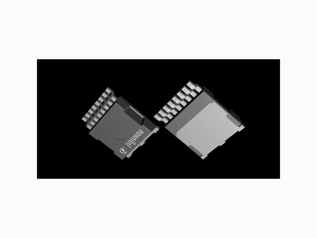
IPTG111N20NM3FD overview
IPTG111N20NM3FD is a component documented by Infineon Technologies A. The PDF description identifies it as "OptiMOSTM 3 Power-Transistor, 200 V Rev. 2.0, 2021-02-11." This guide condenses the most useful engineering information from the available PDF so that designers and sourcing teams can identify the checks that still need confirmation in the original document.
Datasheet snapshot
- Manufacturer: Infineon Technologies A...
- Part number: IPTG111N20NM3FD
- Category: IC
- Datasheet length: 11 Pages
Key features noted in the PDF
- N-channel,normallevel
- Verylowon-resistanceRDS(on)
- Fastdiode(FD)withreducedQrr
- 175°Coperatingtemperature
- Pb-freeleadplating;RoHScompliant
- Halogen-freeaccordingtoIEC61249-2-21
- Optimizedforhardcommutationruggedness Productvalidation FullyqualifiedaccordingtoJEDECforIndustrialApplications Table1KeyPerformanceParameters Parameter Value Unit VDS 200 V RDS(o.
Specifications and operating details
The following points were extracted from the PDF text. Check the associated conditions, notes and limits in the complete document before using a value in a design.
- Parameter Symbol Unit Note/TestCondition Continuous drain current1) ID 108 10.8 A VGS=10V,TC=25°C VGS=10V,TC=100°C VGS=10V,TA=25°C,RTHJA=40°C/W2) Pulsed drain current3) ID,pulse - - 432 A TA=25°C Avalanche energy, single pulse4) EAS - - 37.
- Parameter Symbol Unit Note/TestCondition Thermal resistance, junction - case RthJC - - 0.4 K/W - Thermal resistance, junction - ambient, 6 cm² cooling area RthJA - - 40 K/W - Thermal resistance, junction - ambient, minimal footprint2) RthJ.
- 2) Device on 40 mm x 40 mm x 1.5 mm epoxy PCB FR4 with 6 cm2 (one layer, 70 µm thick) copper area for drain connection.
- 3) See Diagram 3 for more detailed information 4) See Diagram 13 for more detailed information OptiMOSTM3Power-Transistor,200V IPTG111N20NM3FD Rev.2.0,2021-02-11Final Data Sheet 3Electricalcharacteristics atTj=25°C,unlessotherwisespecified.
- Parameter Symbol Unit Note/TestCondition Drain-source breakdown voltage V(BR)DSS 200 - - V VGS=0V,ID=1mA Gate threshold voltage VGS(th) 2 3 4 V VDS=VGS,ID=267µA Zero gate voltage drain current IDSS 0.1 100 µA VDS=160V,VGS=0V,Tj=25°C VDS=16.
- 2) See ″Gate charge waveforms″ for parameter definition OptiMOSTM3Power-Transistor,200V IPTG111N20NM3FD Rev.2.0,2021-02-11Final Data Sheet Table7Reversediode Values Min.
- Parameter Symbol Unit Note/TestCondition Diode continuous forward current IS - - 108 A TC=25°C Diode pulse current IS,pulse - - 432 A TC=25°C Diode forward voltage VSD - 0.95 1.2 V VGS=0V,IF=96A,Tj=25°C Reverse recovery time1) trr - 125 25.
Topics covered by the datasheet
The document includes sections related to:
- Features
Engineering review checklist
- Confirm repetitive reverse voltage, average forward current, surge current and leakage at the intended temperature.
- Check forward-voltage loss and reverse-recovery behavior at the actual current and switching frequency.
- Review package thermal resistance, copper area, polarity marking and transient derating before layout release.
Always confirm values against the latest manufacturer-controlled datasheet, especially when qualifying a substitute or releasing a production BOM.
View the complete PDF and model record
Open the IPTG111N20NM3FD datasheet and model details to review the complete PDF, document pages and available product information.
Source attribution
Adapted from the PDF associated with this DigiCamel model page.
Source model URL: https://www.digicamel.com/product.php?slug=iptg111n20nm3fd-infineon-technologies-a