
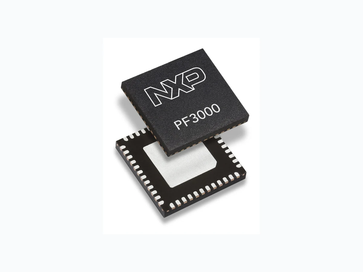
Power management integrated circuit (PMIC) for i.MX 7 & i.MX 6SL/SX/UL
Document overview
- Manufacturer or author: NXP B.V.
- PDF pages: 132
Technical content
Datasheet sections
- 1 General description
- 2 Features and benefits
- 3 Applications
- 4 Ordering information
- 5 Internal block diagram
- 6 Functional block diagram
- 7 Pinning information
- 7.1 Pinning diagram
- 7.2 Pin descriptions
- 8 Functional description
- 8.1 Introduction
- 8.2 Power generation
- 8.3 Functional description
- 8.3.1 Control logic and interface signals
- 8.3.1.1 PWRON
- 8.3.1.2 STANDBY
- 8.3.1.3 RESETBMCU
- 8.3.1.4 INTB
- 8.3.1.5 SD_VSEL
- 8.3.2 OTP memory
- 8.3.2.1 Register naming convention
- 8.3.2.2 Regulator startup sequence programming
- 8.3.2.3 PWRON pin configuration
- 8.3.2.4 I2C address configuration
- 8.3.2.5 Buck regulator soft start ramp rate
- 8.3.3 Startup
- 8.3.3.1 Startup timing diagram
- 8.3.5 Optional front-end input LDO regulator
- 8.3.5.1 LDO regulator description
- 8.3.5.2 Undervoltage/short-circuit and overvoltage
- 8.3.5.3 External components
- 8.3.6 Internal core voltages
- 8.3.7 VREFDDR voltage reference
- 8.3.7.1 VREFDDR external components
- 8.3.8 Buck regulators
- 8.3.8.1 Switching modes
- 8.3.8.2 Dynamic voltage scaling
- 8.3.8.3 Regulator phase clock
- 8.3.8.4 SW1A/B
- 8.3.8.5 SW1A/B single phase
- 8.3.8.6 SW1A – SW1B
- 8.3.8.7 SW1A/B setup and control registers
- 8.3.8.8 SW2 setup and control registers
- 8.3.8.9 SW3 setup and control registers
- 8.3.9 Boost regulator
- 8.3.9.1 SWBST setup and control
- 8.3.9.2 SWBST external components
- 8.3.10 LDO regulators description
- 8.3.10.1 External components
- 8.3.10.2 Current limit protection
- 8.3.10.3 LDO voltage control
- 8.3.11 VSNVS LDO/switch
- 8.3.11.1 VSNVS control
- 8.3.11.2 VSNVS external components
- 8.3.11.3 Coin cell battery backup
- 8.3.11.4 Coin cell charger control
- 8.3.11.5 External components
- 8.4 Power dissipation
- 8.5 Modes of operation
- 8.5.1 State diagram
- 8.5.1.1 On mode
- 8.5.1.2 OFF mode
- 8.5.1.3 PWRON pin
- 8.5.1.4 Thermal protection
- 8.5.1.5 Standby mode
- 8.5.1.6 Sleep/LPSR mode
- 8.5.1.7 Coin Cell mode
- 8.5.2 State machine flow summary
- 8.5.3 Performance characteristics curves
- 8.6 Control interface I2C block description
- 8.6.1 I2C device ID
- 8.6.2 I2C operation
- 8.6.3 Interrupt handling
- 8.6.4 Interrupt bit summary
- 8.6.5 Specific registers
- 8.6.5.1 IC and version identification
- 8.6.5.2 Embedded memory
- 8.6.5.3 Register descriptions
- 8.6.6 Register map
- 8.6.6.1 Register map
- 9 General product characteristics
- 9.1 Absolute maximum ratings
- 9.2 Thermal characteristics
- 9.3 Current consumption
- 9.4 Electrical characteristics
- 10 Typical applications
- 10.1 Application diagram
- 11 Thermal characteristics
- 11.1 Rating data
- 11.2 Estimation of junction temperature
- 12 Bill of materials
- 13 Simplified application diagram
- 14 Package information
- 14.1 Package outline
- 15 Revision history
Power management integrated circuit (PMIC) for i.MX 7 & i.MX 6SL/SX/UL Rev. 10.1 — 9 June 2026 Product data sheet
1 General description
The PF3000 is a power management integrated circuit (PMIC) designed specifically for use with the NXP i.MX 7 and i.MX 6SL/SX/UL application processors. With up to four buck converters, six linear regulators, RTC supply, and coin-cell charger, the PF3000 can provide power for a complete system, including applications processors, memory, and system peripherals. This device is powered by SMARTMOS technology.
2 Features and benefits
This section summarizes the PF3000 features.
- Input voltage range to PMIC: 2.8 V to 4.5 V, or 3.7 V to 5.5 V1 – Buck regulators – Configurable three to four channels – SW1B 1.75 A (independent); 0.7 V to 1.475 V – SW3, 1.5 A; 0.90 V to 1.65 V – Dynamic voltage scaling – Modes: PWM, PFM, APS – Programmable output voltage – Programmable current limit – Programmable soft start sequence – Programmable PWM switching frequency – Boost regulator – SWBST, 5.0 to 5.15 V, 0.6 A, OTG support – Modes: PFM and Auto – OCP fault interrupt – LDOs – VCC_SD, 1.8 V to 1.85 V or 2.85 V to 3.30 V, 100 mA based on SD_VSEL – V33, 2.85 V to 3.30 V, 350 mA – VLDO1, 1.8 V to 3.3 V, 100 mA – VLDO2, 0.80 V to 1.55 V, 250 mA
Power management integrated circuit (PMIC) for i.MX 7 & i.MX 6SL/SX/UL – VLDO3, 1.8 V to 3.3 V, 100 mA – VLDO4, 1.8 V to 3.3 V, 350 mA
- Always-on RTC regulator/switch VSNVS 3.0 V, 1.0 mA
- DDR memory reference voltage, VREFDDR, 0.5 V to 0.9 V, 10 mA
- OTP (one time programmable) memory for device configuration, user-programmable startup sequence and timing
- Battery backed memory including coin cell charger
- I2C interface
- User programmable Standby, Sleep/LPSR, and Off modes
3 Applications
- Tablets
- eReaders
- Wearables
- POS terminals
- Industrial control
- Medical monitoring
- Home automation
- Home security/energy management PF3000 All information provided in this document is subject to legal disclaimers. © 2026 NXP B.V. All rights reserved. Product data sheet Rev. 10.1 — 9 June 2026 Document feedback
4 Ordering information
program codes from Table 1. Details of the OTP programming for each device can be found in Table 10. Table 1. Orderable part variations PF3000 All information provided in this document is subject to legal disclaimers. © 2026 NXP B.V. All rights reserved.
Table 1. Orderable part variations...continued [1] For tape and reel, add an R2 suffix to the part number. design. Table 10 provides details of the OTP programming for each device. [3] The ~EP parts are not recommended for new designs. PF3000 All information provided in this document is subject to legal disclaimers. © 2026 NXP B.V. All rights reserved.
5 Internal block diagram
16 MHz
Figure 1. PF3000 simplified internal block diagram PF3000 All information provided in this document is subject to legal disclaimers. © 2026 NXP B.V. All rights reserved.
6 Functional block diagram
Figure 2. Functional block diagram PF3000 All information provided in this document is subject to legal disclaimers. © 2026 NXP B.V. All rights reserved.
7 Pinning information
7.1 Pinning diagram
Figure 3. Pinning diagram PF3000 All information provided in this document is subject to legal disclaimers. © 2026 NXP B.V. All rights reserved.
7.2 Pin descriptions
1 INTB O Digital Open drain interrupt signal to processor
2 SD_VSEL I/O Digital
- SD_VSEL=0, VCC_SD = 2.85 V to 3.3 V
- SD_VSEL=1, VCC_SD = 1.8 V to 1.85 V
3 RES
4 STANDBY I Digital Standby input signal from processor
5 ICTEST I Digital and
6 SW1AFB[1] I Analog
7 SW1AIN[1] I Analog
8 SW1ALX[1] O Analog
9 SW1BLX[1] O Analog
10 SW1BIN[1] I Analog
11 SW1BFB[1] I Analog
18 SW2IN[1] I Analog
Table 2. Pin descriptions PF3000 All information provided in this document is subject to legal disclaimers. © 2026 NXP B.V. All rights reserved.
19 SW2FB[1] I Analog
24 VIN
26 GNDREF2 GND GND Reference ground for SW2 and SW3 regulators. Connect to GND.
27 SW3FB[1] I Analog
28 SW3IN[1] I Analog
31 VPWR I Analog Input to optional front-end VPWR LDO for systems with input voltage >
38 VIN2 I Analog Input to VCC_SD, V33 regulators and SWBST control circuitry.
39 VDDOTP I Digital &
Table 2. Pin descriptions...continued PF3000 All information provided in this document is subject to legal disclaimers. © 2026 NXP B.V. All rights reserved.
42 VIN I Analog
47 VDDIO I Analog
48 PWRON I Digital Power ON/OFF input from processor
Expose pad. Functions as ground return for buck and boost regulators. VIN with a 0.1 μF bypass capacitor. PF3000 All information provided in this document is subject to legal disclaimers. © 2026 NXP B.V. All rights reserved.
Power management integrated circuit (PMIC) for i.MX 7 & i.MX 6SL/SX/UL
8 Functional description
8.1 Introduction
The PF3000 is any integrated, low-quiescent current power management IC featuring four buck regulators, one boost regulator, seven LDO regulators, and a DDR voltage reference. The PF3000 provides all the necessary rails to power a complete system, including the application processor, memory, and peripherals. The PF3000 operates from an input voltage of up to 5.5 V. Output voltage, startup sequence, and other functions are set using integrated OTP memory, thus providing flexibility and reducing external component count.
8.2 Power generation
The buck regulators in the PF3000 provide supply to the processor cores and to other voltage domains, such as I/O and memory. Dynamic voltage scaling is provided to allow controlled supply rail adjustments for the processor cores and other circuitry. The SW1A and SW1B buck regulators can either be used as independent 1.0 A and 1.75 A regulators, or can be combined as a single 2.75 A regulator. The linear regulators in the PF3000 can be used as general-purpose regulators to power peripherals and lower power processor rails. The VCC_SD LDO regulator supports the dual-voltage requirement by high-speed SD card readers. Depending on the system power path configuration, the LDO regulators can be directly supplied from the main input supply or from the switching regulators to power peripherals, such as audio, camera, Bluetooth, and wireless LAN, and so on. A specific VREFDDR voltage reference is included to provide accurate reference voltage for DDR memories. The VSNVS block behaves as an LDO, or as a bypass switch to supply the SNVS/SRTC circuitry on the i.MX processors; VSNVS may be powered from VIN, or from a coin cell. To accommodate applications that are powered by main supplies of voltages higher than 4.5 V and up to 5.5 V, the PF3000 incorporates a front-end LDO regulator using an external pass FET to keep the maximum regulator input voltage of the regulators at 4.5 V. Applications with an input voltage lower than 4.5 V can directly power the regulators without using the front-end LDO. PF3000 shows a summary of the voltage regulators in the PF3000. PF3000 All information provided in this document is subject to legal disclaimers. © 2026 NXP B.V. All rights reserved. Product data sheet Rev. 10.1 — 9 June 2026 Document feedback
Table 3. PF3000 power tree PF3000 All information provided in this document is subject to legal disclaimers. © 2026 NXP B.V. All rights reserved.
8.3 Functional description
8.3.1 Control logic and interface signals
8.3.1.1 PWRON
PWRON pin can be configured using OTP to detect a level, or an edge using the PWRON_CFG bit.
- If PWRON_CFG = 0, the PWRON signal is high and VIN > UVDET, the PMIC turns on; the interrupt and sense bits, PWRONI and PWRONS respectively, are set.
- If PWRON_CFG = 1, VIN > UVDET and PWRON transitions from high to low, the PMIC turns on; the interrupt and sense bits, PWRONI and PWRONS respectively, are set. Any regulator enabled in Sleep mode remains enabled when transitioning from Sleep to On, that is, the regulator is not turned off and then on again to match the startup sequence. When PWRON_CFG = 1, the PWRON input can be a mechanical switch debounced through a programmable debouncer PWRONDBNC[1:0], to avoid a response to a short key press. The interrupt is generated for both the falling and the rising edges of the PWRON pin. By default, a 31.25 ms interrupt debounce is applied to both falling and rising edges. The falling edge debounce timing can be extended with PWRONDBNC[1:0] as defined in Table 4. The interrupt is cleared by software, or when cycling through Off mode. Bits State Turn-on debounce (ms) Falling edge INT debounce (ms) Rising edge INT debounce (ms) 00 0.0 31.25 31.25 01 31.25 31.25 31.25 10 125 125 31.25 PWRONDBNC[1:0] 11 750 750 31.25
Table 4. PWRON hardware debounce bit settings[1] [1] The sense bit, PWRONS, is not debounced and follows the state of the PWRON pin.
8.3.1.2 STANDBY
does not reliably enter and exit the Standby mode. PF3000 All information provided in this document is subject to legal disclaimers. © 2026 NXP B.V. All rights reserved.
Power management integrated circuit (PMIC) for i.MX 7 & i.MX 6SL/SX/UL
8.3.1.3 RESETBMCU
RESETBMCU is an open-drain, active low output OTP configurable for two modes of operation. In its default mode, it is deasserted 2.0 ms after the last regulator in the startup sequence is enabled. In this mode, the signal can be used to bring the processor out of reset (POR), or as an indicator that all supplies have been enabled; it is only asserted during a turn-off event. In the Default mode, the RESETBMCU signal is internal-timer based and does not monitor the regulators. When configured for its Fault mode, RESETBMCU is deasserted after the startup sequence is completed only if no faults occurred during startup. At any time, if a fault occurs and persists for 1.8 ms, RESETBMCU is asserted Low. The PF3000 is turned off if the fault persists for more than 100 ms. The PWRON signal can be used to restart the part, though if the fault persists, the sequence described above is repeated. To enter Fault mode, set bit OTP_PG_EN of register OTP PWRGD EN to 1 during OTP programming.
8.3.1.4 INTB
INTB is an open drain, active low output. It is asserted when any fault occurs, provided that the fault interrupt is unmasked. INTB is de-asserted after the fault interrupt is cleared by software, which requires writing a 1 to the fault interrupt bit.
8.3.1.5 SD_VSEL
SD_VSEL is an input pin that sets the output voltage range of the VCC_SD regulator. When SD_VSEL = HIGH, the VCC_SD regulator operates in the lower output voltage range. When SD_VSEL = LOW, the VCC_SD regulator operates in the higher output voltage range. The SD_VSEL input buffer is powered by the VDDIO supply. When a valid VDDIO voltage is not present, the output of the SD_VSEL buffer defaults to a logic high, thus keeping the VCC_SD regulator output in the lower voltage range.
8.3.2 OTP memory
OTP memory is used to store key startup parameters and regulators’configuration information. This eliminates the need to set regulator voltage and sequence using external components. The following parameters are programmable in the PF3000. General: I2C follower address, PWRON pin configuration, RESETBMCU configuration Buck regulators: Output Voltage, Single-Phase, or Independent mode configuration for SW1A and SW1B regulators, switching frequency, regulator startup sequence and timing Boost regulator and LDOs: Output voltage, regulator startup sequence and timing The PF3000 starts up based on the contents of the TBBOTP registers. During power up, contents of the OTP memory are loaded onto the TBBOTP registers. There is an optional Try-Before-Buy mode of operation available that bypasses loading of the OTP memory onto the TBBOTP registers. Instead, regulators directly start up based on the current contents of the TBBOTP registers during this mode of operation. This mode is useful when trying to determine a suitable OTP configuration for the system. TBB mode can also be used in lieu of OTP programming provided a microcontroller can initiate the TBB sequence is available in the system.
8.3.2.1 Register naming convention
Register and bit names for the TBBOTP registers are prefixed with OTP. This is to differentiate them from functional registers that are responsible for real-time control of regulator settings. For example, OTP_SW1A_VOLT refers to the TBBOTP register associated with the voltage setting for SW1A regulator. SW1AVOLT refers to the functional register which is fed into the SW1A regulator block. During power up, contents of the OTP fuses are copied onto the OTP_SW1A_VOLT register that is further copied onto the PF3000 All information provided in this document is subject to legal disclaimers. © 2026 NXP B.V. All rights reserved. Product data sheet Rev. 10.1 — 9 June 2026 Document feedback
output voltage of the SW1A regulator. Writes to the SW1AVOLT register do have an effect.
8.3.2.2 Regulator startup sequence programming
each can be placed from position one to seven or one to 15 in the startup sequence as shown in Table 5. be 0.5 ms or 2.0 ms as shown in Table 6. The startup sequence terminates at the last programmed regulator. RESETBMCU pin is deasserted high 2.0 ms after the last utilized startup slot. Table 5. Startup sequence Table 6. Start-up sequence clock speed PF3000 All information provided in this document is subject to legal disclaimers. © 2026 NXP B.V. All rights reserved.
8.3.2.3 PWRON pin configuration
or equal to 4.0 seconds, the part turns off or enters Sleep mode.
0 PWRON pin high = On
1 PWRON pin pulled low momentarily = On
Table 7. PWRON configuration
8.3.2.4 I2C address configuration
Table 8. The I2C address of the PF3000 immediately changes after write instructions to the OTP_I2C_ADDR Table 8. I2C address configuration
8.3.2.5 Buck regulator soft start ramp rate
Table 9. DVS speed selection for SWx PF3000 All information provided in this document is subject to legal disclaimers. © 2026 NXP B.V. All rights reserved.
8.3.3 Startup
fuses during a turn-on event. The PF3000 is available in a number of preprogrammed flavors to suit a wide variety of system configurations.
2.0 MHz
Table 10. Startup configuration [1] internally fixed to be same as SW3_SEQ. VCC_SD voltage depends on the state of the SD_VSEL pin. PF3000 All information provided in this document is subject to legal disclaimers. © 2026 NXP B.V. All rights reserved.
8.3.3.1 Startup timing diagram
V to 3 V. Typically it is 650 μ s. td3 is delay of regulator(s) whose OTP sequence is set to 1. regulator(s). Refer to Table 33. 2 ms with a minimum of 1.8 ms and maximum of 2.2 ms. Figure 5. Startup timing diagram The PF3000 incorporates two clocks: a trimmed 16 MHz RC oscillator and an untrimmed 32 kHz RC oscillator.
- VIN < UVDET
- All regulators are in Sleep mode
- All regulators are in PFM Switching mode A 32 kHz clock, derived from the 16 MHz trimmed clock, is used when accurate timing is needed under the following conditions:
- During startup, VIN > UVDET
- PWRON_CFG = 1, for power button debounce timing When the 16 MHz is active in the On mode, the debounce times are referenced to the 32 kHz derived from the 16 MHz clock. The exceptions are the LOWVINI and PWRONI interrupts, which are referenced to the 32 kHz untrimmed clock. Switching frequency of the switching regulators is derived from the trimmed 16 MHz clock. The 16 MHz clock and, hence the switching frequency of the regulators, can be adjusted to improve the noise integrity of the system. By changing the factory trim values of the 16 MHz clock, the user may add an offset as small as ±3.0% of the nominal frequency. Contact a NXP representative for more information. PF3000 All information provided in this document is subject to legal disclaimers. © 2026 NXP B.V. All rights reserved. Product data sheet Rev. 10.1 — 9 June 2026 Document feedback
8.3.5 Optional front-end input LDO regulator
8.3.5.1 LDO regulator description
operation with supply voltages higher than 4.5 V and up to 5.5 V. voltage of the power FET is changed to maintain a constant output voltage. power consumption. See Section 8.5 for different modes of operation of the IC. Figure 6. Front-end LDO block diagram
8.3.5.2 Undervoltage/short-circuit and overvoltage detection
PF3000 All information provided in this document is subject to legal disclaimers. © 2026 NXP B.V. All rights reserved.
8.3.5.3 External components
Table 11 lists the typical component values for the general purpose LDO regulators. Table 11. Input LDO external components and LDOx inputs to achieve a total of 100 μF capacitance.
8.3.6 Internal core voltages
powered as long as there is a valid supply and/or valid coin cell.
8.3.7 VREFDDR voltage reference
Figure 7. VREFDDR block diagram PF3000 All information provided in this document is subject to legal disclaimers. © 2026 NXP B.V. All rights reserved.
8.3.7.1 VREFDDR external components
Table 12. VREFDDR external components [1] [1] Use X5R or X7R capacitors. [2] VINREFDDR to GND, 1.0 μF minimum capacitance is provided by buck regulator output.
8.3.8 Buck regulators
Figure 8. Generic SWx block diagram Table 13. SWx regulators external components Note: Use X5R or X7R capacitors with voltage rating at least two times the nominal voltage. PF3000 All information provided in this document is subject to legal disclaimers. © 2026 NXP B.V. All rights reserved.
8.3.8.1 Switching modes
OFF The regulator is switched off and the output voltage is discharged using an internal resistor. PWM In this mode, the regulator operates in forced PWM mode. Table 14. Switching mode description summarizes the buck regulator programmability for Normal and Standby modes.
0000 Off Off
0001 PWM Off
0010 Reserved Reserved
0011 PFM Off
0100 APS Off
0101 PWM PWM
0110 PWM APS
0111 Reserved Reserved
1001 Reserved Reserved
1010 Reserved Reserved
1011 Reserved Reserved
1100 APS PFM
1101 PWM PFM
1110 Reserved Reserved
1111 Reserved Reserved
Table 15. Regulator mode control PF3000 All information provided in this document is subject to legal disclaimers. © 2026 NXP B.V. All rights reserved.
returns to its normal Switching mode and its output voltage programmed in its voltage register. regulator returns to its default On state output voltage and switch mode settings. SW1xOFF[4:0] for SW1A/B and by SW2OFF[2:0] for SW2, and SW3OFF[3:0] for SW3.
8.3.8.2 Dynamic voltage scaling
- Normal operation: The output voltage is selected by I2C bits SW1x[4:0] for SW1A/B and SW2[2:0] for SW2,
- Standby mode: The output voltage can be selected by I2C bits SW1xSTBY[4:0] for SW1A/B and by bits
governed by the DVS stepping rates shown in Table 16.
- Sleep mode: The output voltage can be higher or lower than in normal operation, but is typically selected
turn-off event are governed by the DVS stepping rates shown in Table 16. Table 16. DVS speed selection for SWx programmed in PFM or APS mode during a DVS transition, the falling slope can be influenced by the load. be affected. Critically timed DVS transitions are best assured with PWM mode operation. Figure 9 shows the general behavior for the regulators when initiated with I2C programming, or standby control. During the DVS period, the overcurrent condition on the regulator should be masked. PF3000 All information provided in this document is subject to legal disclaimers. © 2026 NXP B.V. All rights reserved.
Figure 9. Voltage stepping with DVS voltage settings is not allowed.
8.3.8.3 Regulator phase clock
is set to 90 °C, and SW3 is set to 180 °C by default at power up. Table 17. Regulator phase clock selection The SWxFREQ[1:0] register is used to set the desired switching frequency for each one of the buck regulators. phasing. Table 18 shows the optimum phasing when using more than one switching frequency.
1.0 MHz
4.0 MHz
Table 18. Optimum phasing PF3000 All information provided in this document is subject to legal disclaimers. © 2026 NXP B.V. All rights reserved.
11 Reserved
Table 19. Regulator frequency configuration
8.3.8.4 SW1A/B
- SW1A/B single phase with one inductor
- SW1A in independent with one inductor and SW1B in Independent mode with a second inductor The desired configuration is programmed by OTP by using OTP_SW1_CONFIG[1:0] bits in the register map, as shown in Table 20. OTP_SW1_CONFIG[1:0] Description
00 Unused
01 A/B Single phase
10 Unused
11 A Independent mode
Table 20. SW1 configuration
8.3.8.5 SW1A/B single phase
SW1BFB pin should be left floating in this configuration. Figure 10. SW1A/B single phase diagram PF3000 All information provided in this document is subject to legal disclaimers. © 2026 NXP B.V. All rights reserved.
8.3.8.6 SW1A – SW1B
mode selection and on/off control.
8.3.8.7 SW1A/B setup and control registers
programming by setting the OTP_SW1A_VOLT and OTP_SW1B_VOLT registers, appropriately. Table 21. SW1A/B output voltage configuration PF3000 All information provided in this document is subject to legal disclaimers. © 2026 NXP B.V. All rights reserved.
Table 22 provides a list of registers used to configure and operate SW1A/B regulator(s). Table 22. SW1A/B register summary
8.3.8.8 SW2 setup and control registers
bits, respectively. Table 23 shows the output voltage coding valid for SW2. Table 23. SW2 output voltage configuration PF3000 All information provided in this document is subject to legal disclaimers. © 2026 NXP B.V. All rights reserved.
Setup and control of SW2 is done through the I2C registers listed in Table 24. Table 24. SW2 register summary
8.3.8.9 SW3 setup and control registers
memory as listed in Table 25. Table 25. SW3 output voltage configuration Table 26 provides a list of registers used to configure and operate SW3. Table 26. SW3 register summary
8.3.9 Boost regulator
regulator for the USB PHY in OTG mode, as well as the VBUS voltage. PF3000 All information provided in this document is subject to legal disclaimers. © 2026 NXP B.V. All rights reserved.
Figure 11 shows the block diagram and component connection for the boost regulator. Figure 11. Boost regulator architecture
8.3.9.1 SWBST setup and control
in the power-up sequence if its OTP power-up timing bits, OTP_SWBST_SEQ[2:0], are not all zeros. Table 27. Register SWBSTCTL - ADDR 0x66 enabled in the startup sequence. enabled in the startup sequence. PF3000 All information provided in this document is subject to legal disclaimers. © 2026 NXP B.V. All rights reserved.
8.3.9.2 SWBST external components
Table 28. SWBST external component requirements [1] Use X5R or X7R capacitors.
8.3.10 LDO regulators description
reference. When a regulator is disabled, the output is discharged by an internal pulldown resistor. Figure 12. General LDO block diagram
8.3.10.1 External components
Section 8.3 lists the typical component values for the general purpose LDO regulators. Table 29. LDO external components [1] Use X5R/X7R ceramic capacitors. PF3000 All information provided in this document is subject to legal disclaimers. © 2026 NXP B.V. All rights reserved.
8.3.10.2 Current limit protection
condition regardless of the state of the REGSCPEN bit.
8.3.10.3 LDO voltage control
OTP_VLDO_VOLT register is copied to the VLDOxCTL registers. Table 30. VLDO1, VLDO2 output voltage configuration PF3000 All information provided in this document is subject to legal disclaimers. © 2026 NXP B.V. All rights reserved.
Table 31. VLDO3, VLDO4 output voltage configuration Table 32. V33 output voltage configuration Table 33. VCC_SD output voltage configuration bits on VLDOxCTL register and the expected behavior of the LDO output. PF3000 All information provided in this document is subject to legal disclaimers. © 2026 NXP B.V. All rights reserved.
0 X X X Off
1 X 1 0 On
Table 34. LDO control [1] STANDBY refers to a standby event as described earlier.
8.3.11 VSNVS LDO/switch
which is 100 mV at a rated maximum load current of 1000 μA. changes configuration from an LDO to a switch, provided certain conditions are met as described in Table 35.
2.25 V (VTL0) -
Figure 13. VSNVS supply switch architecture Table 35. SNVS modes of operation PF3000 All information provided in this document is subject to legal disclaimers. © 2026 NXP B.V. All rights reserved.
8.3.11.1 VSNVS control
Table 36. Register VSNVSCTL - ADDR 0x6B [1] Only valid when a valid input voltage is present.
8.3.11.2 VSNVS external components
Table 37. VSNVS external components
8.3.11.3 Coin cell battery backup
8.3.11.4 Coin cell charger control
stopped when VIN is below UVDET. Table 38. Coin cell charger voltage PF3000 All information provided in this document is subject to legal disclaimers. © 2026 NXP B.V. All rights reserved.
Table 38. Coin cell charger voltage ...continued [1] Coin cell voltages selected based on the type of LICELL used on the system. VCOIN 2:0 R/W 0x00 Coin cell charger output voltage selection. Table 39. Register COINCTL - ADDR 0x1A
8.3.11.5 External components
Table 40. Coin cell charger external components
8.4 Power dissipation
Table 41. Thermal protection thresholds PF3000 All information provided in this document is subject to legal disclaimers. © 2026 NXP B.V. All rights reserved.
8.5 Modes of operation
8.5.1 State diagram
The operation of the PF3000 can be reduced to five states, or modes: On, Off, Sleep, Standby, and Coin Cell. Figure 14 shows the state diagram of the PF3000, along with the conditions to enter and exit from each state. Figure 14. State diagram To complement the state diagram in Figure 14, a description of the states is provided in following sections. Note: VIN must exceed the rising UVDET threshold to allow a power up. interrupt signal, INTB, is only active in Sleep, Standby, and On states.
8.5.1.1 On mode
undervoltage falling threshold, UVDET, the state machine transitions to the Coin Cell mode. PF3000 All information provided in this document is subject to legal disclaimers. © 2026 NXP B.V. All rights reserved.
8.5.1.2 OFF mode
of operation. To exit the Off mode, a valid turn-on event is required. RESETBMCU is asserted low, in this mode. Turn off events can be achieved using the PWRON pin, thermal protection, as described below.
8.5.1.3 PWRON pin
- PWRON_CFG bit = 0, SWxOMODE bit = 0 and PWRON pin is low.
- PWRON_CFG bit = 1, SWxOMODE bit = 0, PWRONRSTEN = 1 and PWRON is held low for longer than
8.5.1.4 Thermal protection
8.5.1.5 Standby mode
- Depending on STANDBY pin configuration, Standby is entered when the STANDBY pin is asserted. This is typically used for Low-Power mode of operation.
- When STANDBY is deasserted, Standby mode is exited. A product may be designed to go into a Low-Power mode after periods of inactivity. The STANDBY pin is provided for board-level control of going in and out of such Deep Sleep modes (DSM). When a product is in DSM, it may be able to reduce the overall platform current by lowering the regulator output voltage, changing the operating mode of the regulators or disabling some regulators. The configuration of the regulators in standby is pre-programmed through the I2C interface. Note: The STANDBY pin is programmable for active high or active low polarity, and that decoding of a standby event takes into account the programmed input polarity as shown in Table 42. When the PF3000 is powered up first, regulator settings for the Standby mode are mirrored from the regulator settings for the On mode. To change the STANDBY pin polarity to active low, set the STANDBYINV bit via software first, and then change the regulator settings for Standby mode as required. For simplicity, STANDBY is generally referred to as active high throughout this document. STANDBY (Pin)[1] STANDBYINV (I2C bit)[2] STANDBY Control[3] 0 0 0 0 1 1 1 0 1 1 1 0
Table 42. Standby pin and polarity control [2] The state of the STANDBY pin only has influence in On mode. PF3000 All information provided in this document is subject to legal disclaimers. © 2026 NXP B.V. All rights reserved.
received to terminate processes to facilitate seamless entering into Standby mode. required to synchronize the standby event.
00 No delay
01 One 32 kHz period (default)
10 Two 32 kHz periods
11 Three 32 kHz periods
Table 43. STANDBY delay - initiated response
8.5.1.6 Sleep/LPSR mode
- Depending on PWRON pin configuration, Sleep mode is entered when PWRON is deasserted and SWxOMODE bit is set.
- To exit Sleep mode, assert the PWRON pin. In Sleep mode, the regulator uses the set point as programmed by SW1xOFF[3:0] for SW1A/B and by SWxOFF[2:0] for SW2 and SW3. The activated regulators maintain settings for this mode and voltage until the next turn-on event. Table 44 shows the control bits in Sleep mode. During Sleep mode, interrupts are active and the INTB pin reports any unmasked fault event. If LPSR is activated by requesting VDD_LPSR and VCC_GPIO to stay ON, LDO1, and LDO3 enables in Low-Power mode. SWxOMODE Off Operational mode (sleep)[1]
0 Off
1 PFM
Table 44. Regulator mode control SW2, and SW3OFF[3:0] for SW3.
8.5.1.7 Coin Cell mode
on COINPORB are restored to their default states. PF3000 All information provided in this document is subject to legal disclaimers. © 2026 NXP B.V. All rights reserved.
8.5.2 State machine flow summary
Table 45. State machine flow summary PF3000 All information provided in this document is subject to legal disclaimers. © 2026 NXP B.V. All rights reserved.
8.5.3 Performance characteristics curves
Figure 15. Typical startup waveforms Figure 16. Load transient response - LDO1, LDO3 and VCC_SD Figure 17. Load transient response - LDO2 PF3000 All information provided in this document is subject to legal disclaimers. © 2026 NXP B.V. All rights reserved.
Figure 31. Dropout voltage - VLDO4, V33 - VOUT = 3.3 V Figure 32. Dropout voltage - VLDO4 - VOUT = 1.8 V
8.6 Control interface I2C block description
information about how the IC is operating. controller via software. It is recommended to use a drive strength of 80 Ω or higher to increase the edge times. use 5.1 pF capacitors from SCL and SDA to ground for bus pullup resistors of 4.8 kΩ. PF3000 All information provided in this document is subject to legal disclaimers. © 2026 NXP B.V. All rights reserved.
8.6.1 I2C device ID
8.6.2 I2C operation
The I2C interface is configured as follower. with the MSB and each byte is sent out unless a STOP command or NACK is received prior to completion. any time a NACK is received, the host should terminate the current transaction and retry the transaction. The PF3000 uses the repeated start operation for reads as shown in Figure 34. Figure 33. Data transfer on the I2C bus Figure 34. Read operation PF3000 All information provided in this document is subject to legal disclaimers. © 2026 NXP B.V. All rights reserved.
8.6.3 Interrupt handling
an existing interrupt bit, the INTB pin remains low. all interrupts masked, so the processor must initially poll the device to determine if any interrupts are active. the INTB pin goes low after unmasking. asynchronous nature of the debounce timer, the effective debounce time can vary slightly.
8.6.4 Interrupt bit summary
behavioral descriptions, see the related chapters.
2.70 V threshold
Table 46. Interrupt, mask, and sense bits PF3000 All information provided in this document is subject to legal disclaimers. © 2026 NXP B.V. All rights reserved.
Table 46. Interrupt, mask, and sense bits ...continued [1] Debounce timing for the falling edge can be extended with PWRONDBNC[1:0]. A full description of all interrupt, mask, and sense registers is provided in Table 47 to Table 58. Table 47. Register INTSTAT0 – ADDR 0x05 PF3000 All information provided in this document is subject to legal disclaimers. © 2026 NXP B.V. All rights reserved.
Table 48. Register INTMASK0 – ADDR 0x06 Table 49. Register INTSENSE0 – ADDR 0x07 Table 50. Register INTSTAT1 – ADDR 0x08 PF3000 All information provided in this document is subject to legal disclaimers. © 2026 NXP B.V. All rights reserved.
Table 50. Register INTSTAT1 – ADDR 0x08...continued Table 51. Register INTMASK1 – ADDR 0x09 Table 52. Register INTSENSE1 – ADDR 0x0A PF3000 All information provided in this document is subject to legal disclaimers. © 2026 NXP B.V. All rights reserved.
grounded and the VIN path is used to power the PF3000. Table 53. Register INTSTAT3 – ADDR 0x0E Table 54. Register INTMASK3 – ADDR 0x0F TBB registers while this bit is 1. Table 55. Register INTSENSE3 – ADDR 0x10 Table 56. Register INTSTAT4 – ADDR 0x11 PF3000 All information provided in this document is subject to legal disclaimers. © 2026 NXP B.V. All rights reserved.
Table 56. Register INTSTAT4 – ADDR 0x11...continued Table 57. Register INTMASK4 – ADDR 0x12 Table 58. Register INTSENSE4 – ADDR 0x13 PF3000 All information provided in this document is subject to legal disclaimers. © 2026 NXP B.V. All rights reserved.
8.6.5 Specific registers
8.6.5.1 IC and version identification
described in Table 59 to Table 61. Table 59. Register DEVICEID – ADDR 0x00 Table 60. Register SILICON REV – ADDR 0x03 Table 61. Register FABID – ADDR 0x04
8.6.5.2 Embedded memory
discharged, removed, or contact-bounced. The contents of the embedded memory are reset by COINPORB. The banks can be used for any system need for bit retention with coin cell backup. Table 62. Register MEMA – ADDR 0x1C Table 63. Register MEMB – ADDR 0x1D PF3000 All information provided in this document is subject to legal disclaimers. © 2026 NXP B.V. All rights reserved.
Table 64. Register MEMC – ADDR 0x1E Table 65. Register MEMD – ADDR 0x1F
8.6.5.3 Register descriptions
8.6.5.3.1 Interrupt status register 0 (INTSTAT0)
Table 66. Status interrupt register 0 (INTSTAT0) 0 Die temperature has not crossed THERM130 threshold. 1 Die temperature has crossed THERM130 threshold. 0 Die temperature has not crossed THERM125 threshold. 1 Die temperature has crossed THERM125 threshold. 0 Die temperature has not crossed THERM120 threshold. 1 Die temperature has crossed THERM120 threshold. Table 67. INTSTAT0 field descriptions PF3000 All information provided in this document is subject to legal disclaimers. © 2026 NXP B.V. All rights reserved.
0 Die temperature has not crossed THERM110 threshold. 1 Die temperature has crossed THERM110 threshold. can only be cleared by writing a 1. Writing a 0 has no effect. cleared by writing a 1. Writing a 0 has no effect. 0 Power on has not occurred. Table 67. INTSTAT0 field descriptions...continued
8.6.5.3.2 Interrupt status mask register 0 (INTMASK0)
corresponding interrupt. When unmasked, the corresponding interrupt state is reflected on the INTB pin. Table 68. Interrupt status mask register 0 (INTMASK0)
0 THERM130I unmasked
1 THERM130I Masked
0 THERM125I unmasked
1 THERM125I masked
0 THERM120I unmasked
1 THERM120I masked
0 THERM110I unmasked
1 THERM110I masked
0 LOWVINI unmasked
1 LOWVINI masked
Table 69. INTMASK0 field descriptions PF3000 All information provided in this document is subject to legal disclaimers. © 2026 NXP B.V. All rights reserved.
0 PWRONI unmasked
1 PWRONI masked
Table 69. INTMASK0 field descriptions...continued
8.6.5.3.3 Interrupt sense register 0 (INTSENSE0)
Table 70. Interrupt sense register 0 (INTSENSE0) [2] Default value depends on the initial VDDOTP pin state. [3] Default value depends on the initial temperature of the die. [4] Default value depends on the initial VIN voltage. [5] Default value depends on the initial PWRON pin state. 1 VDDOTP to VCOREDIG or greater. 0 Die temperature below THERM130 threshold. 1 Die temperature above THERM130 threshold. 0 Die temperature below THERM125 threshold. 1 Die temperature has crossed THERM125 threshold. 0 Die temperature below THERM120 threshold. 1 Die temperature has crossed THERM120 threshold. 0 Die temperature below THERM110 threshold. 1 Die temperature has crossed THERM110 threshold.
0 PWRON low
1 PWRON high
Table 71. INTSENSE0 field descriptions PF3000 All information provided in this document is subject to legal disclaimers. © 2026 NXP B.V. All rights reserved.
8.6.5.3.4 Interrupt status register 1 (INTSTAT1)
Table 72. Status interrupt register 1 (INTSTAT1) protection. This flag can only be cleared by writing a 1. Writing a 0 has no effect.
0 SW3 in normal operation
1 SW3 above current limit
protection. This flag can only be cleared by writing a 1. Writing a 0 has no effect.
0 SW2 in normal operation
1 SW2 above current limit
limit protection. This flag can only be cleared by writing a 1. Writing a 0 has no effect.
0 SW1B in normal operation
1 SW1B above current limit
limit protection. This flag can only be cleared by writing a 1. Writing a 0 has no effect.
0 SW1A in normal operation
1 SW1A above current limit
Table 73. INTSTAT1 field descriptions
8.6.5.3.5 Interrupt status mask register 1 (INTMASK1)
corresponding interrupt. When unmasked, the corresponding interrupt state is reflected on the INTB pin. Table 74. Interrupt status mask register 1 (INTMASK1) PF3000 All information provided in this document is subject to legal disclaimers. © 2026 NXP B.V. All rights reserved.
0 SW3FAULTI Unmasked
1 SW3FAULTI Masked
0 SW2FAULTI Unmasked
1 SW2FAULTI Masked
0 SW1BFAULTI Unmasked
1 SW1BFAULTI Masked
0 SW1AFAULTI Unmasked
1 SW1AFAULTI Masked
Table 75. INTMASK1 field descriptions
8.6.5.3.6 Interrupt sense register 1 (INTSENSE1)
Table 76. Interrupt sense register 1 (INTSENSE1) Table 77. INTSENSE1 field descriptions PF3000 All information provided in this document is subject to legal disclaimers. © 2026 NXP B.V. All rights reserved.
8.6.5.3.7 Interrupt status register 3 (INTSTAT3)
Table 78. Status Interrupt Register 3 (INTSTAT3) can only be cleared by writing a 1. Writing a 0 has no effect.
0 No error detected
1 OTP error detected
sequence is completed. This flag can only be cleared by writing a 1. Writing a 0 has no effect.
0 OTP auto fuse blow sequence not completed
1 OTP auto fuse blow sequence completed
circuit. This flag can only be cleared by writing a 1. Writing a 0 has no effect. 0 VPWR in normal operation range. 1 VPWR in overvoltage range. current limit protection. This flag can only be cleared by writing a 1. Writing a 0 has no effect.
0 SWBST in normal operation
1 SWBST above current limit
Table 79. INTSTAT3 field descriptions PF3000 All information provided in this document is subject to legal disclaimers. © 2026 NXP B.V. All rights reserved.
8.6.5.3.8 Interrupt status mask register 3 (INTMASK3)
corresponding interrupt. When unmasked, the corresponding interrupt state is reflected on the INTB pin. Table 80. Interrupt status mask register 3 (INTMASK3)
0 OTP_ECCI Unmasked
1 OTP_ECCI Masked
0 OTP_AUTO_BLOW_DONEI Unmasked
1 OTP_AUTO_BLOW_DONEI Masked
0 VPWROVI Unmasked
1 VPWROVI Masked
0 SWBSTFAULTI Unmasked
1 SWBSTFAULTI Masked
Table 81. INTMASK3 field descriptions
8.6.5.3.9 Interrupt sense register 3 (INTSENSE3)
Table 82. Interrupt sense register 3 (INTSENSE3) PF3000 All information provided in this document is subject to legal disclaimers. © 2026 NXP B.V. All rights reserved.
the OTP TBB registers while this bit is 1.
1 SW2 at current limit
0 VPWR in normal operation range. 1 VPWR in overvoltage range. Table 83. INTSENSE3 field descriptions
8.6.5.3.10 Interrupt status register 4 (INTSTAT4)
Table 84. Status interrupt register 4 (INTSTAT4) limit protection. This flag can only be cleared by writing a 1. Writing a 0 has no effect.
0 VLDO4 in normal operation
1 VLDO4 above current limit
limit protection. This flag can only be cleared by writing a 1. Writing a 0 has no effect.
0 VLDO3 in normal operation
1 VLDO3 above current limit
protection. This flag can only be cleared by writing a 1. Writing a 0 has no effect.
0 V33 in normal operation
1 V33 above current limit
current limit protection. This flag can only be cleared by writing a 1. Writing a 0 has no effect.
0 VCC_SD in normal operation
1 VCC_SD above current limit
Table 85. INTSTAT4 field descriptions PF3000 All information provided in this document is subject to legal disclaimers. © 2026 NXP B.V. All rights reserved.
limit protection. This flag can only be cleared by writing a 1. Writing a 0 has no effect. 0 VLDO2 in normal operation range.
1 VLDO2 above current limit
current limit protection. This flag can only be cleared by writing a 1. Writing a 0 has no effect. 0 VLDO1 in normal operation range.
1 VLDO1 above current limit
Table 85. INTSTAT4 field descriptions...continued
8.6.5.3.11 Interrupt status mask register 4 (INTMASK4)
corresponding interrupt. When unmasked, the corresponding interrupt state is reflected on the INTB pin. Table 86. Interrupt status mask register 4 (INTMASK4)
0 VLDO4FAULTI Unmasked
1 VLDO4FAULTI Masked
0 VLDO3FAULTI Unmasked
1 VLDO3FAULTI Masked
0 V33FAULTI Unmasked
1 V33FAULTI Masked
0 VCC_SDFAULTI Unmasked
1 VCC_SDFAULTI Masked
0 VLDO2FAULTI Unmasked
1 VLDO2FAULTI Masked
0 VLDO1FAULTI Unmasked
1 VLDO1FAULTI Masked
Table 87. INTMASK4 field descriptions PF3000 All information provided in this document is subject to legal disclaimers. © 2026 NXP B.V. All rights reserved.
8.6.5.3.12 Interrupt sense register 4 (INTSENSE4)
Table 88. Interrupt sense register 4 (INTSENSE4)
0 VLDO2 in normal operation
0 VLDO1 in normal operation
Table 89. INTSENSE4 Field Descriptions PF3000 All information provided in this document is subject to legal disclaimers. © 2026 NXP B.V. All rights reserved.
8.6.5.3.13 Coin cell control register (COINCTL)
This register is used to control the coin cell charger. Table 90. Coin cell control register (COINCTL) 0 Coin cell charger disabled. 1 Coin cell charger enabled. from 2.50 V to 3.30 V. See Table 38 for all options selectable through these bits. Table 91. COINCTL field descriptions
8.6.5.3.14 Power control register (PWRCTL)
Table 92. Power control register (PWRCTL) occurs on a LDO regulator, this regulator is shutdown.
0 Short-circuit protection disabled
1 Short-circuit protection enabled
STANDBY inversion bit — STANDBYINV is used to control the polarity of the STANDBY pin.
0 STANDBY pin is active high
1 STANDBY pin is active low
Table 93. PWRCTL field descriptions PF3000 All information provided in this document is subject to legal disclaimers. © 2026 NXP B.V. All rights reserved.
STANDBY pin and the entering in Standby mode. PWRON input pin. For configuration, see Table 4.
0 Disallow Off mode after PWRON held low
1 Allow Off mode after PWRON held low
generated by the PWRON (held low for 4 seconds or longer) when PWR_CFG bit = 1.
0 Automatic restart disabled
1 Automatic restart enabled
Table 93. PWRCTL field descriptions...continued
8.6.5.3.15 Embedded memory register A (MEMA)
Table 94. Embedded memory register A (MEMA) present. The contents of the embedded memory are reset by COINPORB. Table 95. MEMA field descriptions PF3000 All information provided in this document is subject to legal disclaimers. © 2026 NXP B.V. All rights reserved.
8.6.5.3.16 Embedded memory register B (MEMB)
Table 96. Embedded memory register B (MEMB) present. The contents of the embedded memory are reset by COINPORB. Table 97. MEMB field descriptions
8.6.5.3.17 Embedded memory register C (MEMC)
Table 98. Embedded Memory Register C (MEMC) present. The contents of the embedded memory are reset by COINPORB. Table 99. MEMC field descriptions PF3000 All information provided in this document is subject to legal disclaimers. © 2026 NXP B.V. All rights reserved.
8.6.5.3.18 Embedded memory register D (MEMD)
Table 100. Embedded memory register D (MEMD) present. The contents of the embedded memory are reset by COINPORB. Table 101. MEMD field descriptions
8.6.5.3.19 SW1A voltage control register (SW1AVOLT)
This register is used to set the output voltage of the SW1A regulator in normal operation. Table 102. SW1A voltage control register (SW1AVOLT) [2] Default value depends on OTP content. Table 103. SW1AVOLT field descriptions PF3000 All information provided in this document is subject to legal disclaimers. © 2026 NXP B.V. All rights reserved.
8.6.5.3.20 SW1A standby voltage control register (SW1ASTBY)
This register is used to set the output voltage of the SW1A regulator in standby operation. Table 104. SW1A standby voltage control register (SW1ASTBY) [2] Default value depends on OTP content. Table 105. SW1ASTBY field descriptions
8.6.5.3.21 SW1A sleep mode voltage control register (SW1AOFF)
This register is used to set the output voltage of the SW1A regulator in Sleep mode operation. Table 106. SW1A Sleep mode voltage control register (SW1AOFF) [2] Default value depends on OTP content. Table 107. SW1AOFF field descriptions PF3000 All information provided in this document is subject to legal disclaimers. © 2026 NXP B.V. All rights reserved.
8.6.5.3.22 SW1A Switching mode selector register (SW1AMODE)
This register is used to set the Switching mode of the SW1A regulator. Table 108. SW1A Switching mode selector register (SW1AMODE) [2] Default value depends on OTP content.
0 OFF mode entered after a turn-off event
1 Sleep mode entered after a turn-off event
Table 109. SW1AMODE field descriptions
8.6.5.3.23 SW1A configuration register (SW1ACONF)
Table 110. SW1A configuration register (SW1ACONF) [2] Default value depends on OTP content. SW1A DVS speed bit — This bit configures the DVS stepping rates speed for SW1A. See Table 16. SW1APHASE SW1A phase clock bit — SW1APHASE is used to set the phase clock for SW1A. See Table 17. Table 111. SW1ACONF field descriptions PF3000 All information provided in this document is subject to legal disclaimers. © 2026 NXP B.V. All rights reserved.
SW1A current limiter bit — This bit configures the current limit for SW1A. Table 111. SW1ACONF field descriptions...continued
8.6.5.3.24 SW1B voltage control register (SW1BVOLT)
This register is used to set the output voltage of the SW1B regulator in normal operation. Table 112. SW1B voltage control register (SW1BVOLT) [2] Default value depends on OTP content. SW1B SW1B output voltage — See Table 21. Table 113. SW1BVOLT field descriptions
8.6.5.3.25 SW1B standby voltage control register (SW1BSTBY)
This register is used to set the output voltage of the SW1B regulator in standby operation. Table 114. SW1B standby voltage control register (SW1BSTBY) [2] Default value depends on OTP content. PF3000 All information provided in this document is subject to legal disclaimers. © 2026 NXP B.V. All rights reserved.
SW1BSTBY SW1B standby output voltage — See Table 21. Table 115. SW1BSTBY field descriptions
8.6.5.3.26 SW1B Sleep mode voltage control register (SW1BOFF)
This register is used to set the output voltage of the SW1B regulator in Sleep mode operation. Table 116. SW1B Sleep mode voltage control register (SW1BOFF) [2] Default value depends on OTP content. SW1BSTBY SW1B Sleep mode output voltage — See Table 21. Table 117. SW1BOFF field descriptions
8.6.5.3.27 SW1B Switching mode selector register (SW1BMODE)
This register is used to set the Switching mode of the SW1B regulator. Table 118. SW1B Switching mode selector register (SW1BMODE) [2] Default value depends on OTP content. Table 119. SW1BMODE field descriptions PF3000 All information provided in this document is subject to legal disclaimers. © 2026 NXP B.V. All rights reserved.
SW1BMODE SW1B Switching mode selector — See Table 15. Table 119. SW1BMODE field descriptions...continued
8.6.5.3.28 SW1B configuration register (SW1BCONF)
Table 120. SW1B configuration register (SW1BCONF) [2] Default value depends on OTP content. SW1B DVS speed bit — This bit configures the DVS stepping rates speed for SW1B. See Table 16. SW1BPHASE SW1B phase clock bit — SW1BPHASE is used to set the phase clock for SW1B. See Table 17. SW1B current limiter bit — This bit configures the current limit for SW1B. Table 121. SW1BCONF field descriptions
8.6.5.3.29 SW2 voltage control register (SW2VOLT)
This register is used to set the output voltage of the SW2 regulator in normal operation. Table 122. SW2 voltage control register (SW2VOLT) [2] Default value depends on OTP content. PF3000 All information provided in this document is subject to legal disclaimers. © 2026 NXP B.V. All rights reserved.
SW2 SW2 output voltage — See Table 23. SW2 output voltage range —This bit configures the range of SW2 output voltage. See Table 23.
0 Low output voltage settings
1 High output voltage settings
Table 123. SW2VOLT field descriptions
8.6.5.3.30 SW2 standby voltage control register (SW2STBY)
This register is used to set the output voltage of the SW2 regulator in standby operation. Table 124. SW2 standby voltage control register (SW2STBY) [2] Default value depends on OTP content. SW2STBY SW2 standby output voltage — See Table 23. SW2 output voltage range —This bit configures the range of SW2 output voltage. See Table 23. Table 125. SW2STBY field descriptions
8.6.5.3.31 SW2 Sleep mode voltage control register (SW2OFF)
This register is used to set the output voltage of the SW2 regulator in Sleep mode operation. Table 126. SW2 Sleep mode voltage control register (SW2OFF) [2] Default value depends on OTP content. PF3000 All information provided in this document is subject to legal disclaimers. © 2026 NXP B.V. All rights reserved.
SW2STBY SW2 sleep mode output voltage — See Table 23. SW2 output voltage range — This bit configures the range of SW2 output voltage. See Table 23. Table 127. SW2OFF field descriptions
8.6.5.3.32 SW2 Switching mode selector register (SW2MODE)
This register is used to set the Switching mode of the SW2 regulator. Table 128. SW2 Switching mode selector register (SW2MODE) [2] Default value depends on OTP content. SW2MODE SW2 switching mode selector — See Table 15. Table 129. SW2MODE field descriptions
8.6.5.3.33 SW2 configuration register (SW2CONF)
Table 130. SW2 configuration register (SW2CONF) [2] Default value depends on OTP content. PF3000 All information provided in this document is subject to legal disclaimers. © 2026 NXP B.V. All rights reserved.
SW2 DVS speed bit — This bit configures the DVS stepping rates speed for SW2. See Table 16. SW2PHASE SW2 phase clock bit — SW2PHASE is used to set the phase clock for SW2. See Table 17. SW2 switching frequency — SW2PHASE is used to set the desired switching frequency for SW2. SW2 current limiter bit — This bit configures the current limit for SW2. Table 131. SW2CONF field descriptions
8.6.5.3.34 SW3 voltage control register (SW3VOLT)
This register is used to set the output voltage of the SW3 regulator in normal operation. Table 132. SW3 voltage control register (SW3VOLT) [2] Default value depends on OTP content. SW3 SW3 output voltage — See Table 25. Table 133. SW3VOLT field descriptions
8.6.5.3.35 SW3 standby voltage control register (SW3STBY)
This register is used to set the output voltage of the SW3 regulator in standby operation. Table 134. SW3 standby voltage control register (SW3STBY) [2] Default value depends on OTP content. PF3000 All information provided in this document is subject to legal disclaimers. © 2026 NXP B.V. All rights reserved.
SW3STBY SW3 standby output voltage — See Table 25. Table 135. SW3STBY field descriptions
8.6.5.3.36 SW3 Sleep mode voltage control register (SW3OFF)
This register is used to set the output voltage of the SW3 regulator in Sleep mode operation. Table 136. SW3 Sleep mode voltage control register (SW3OFF) [2] Default value depends on OTP content. SW3STBY SW3 Sleep mode output voltage — See Table 25. Table 137. SW3OFF field descriptions
8.6.5.3.37 SW3 Switching mode selector register (SW3MODE)
This register is used to set the Switching mode of the SW3 regulator. Table 138. SW3 Switching mode selector register (SW3MODE) [2] Default value depends on OTP content. Table 139. SW3MODE field descriptions PF3000 All information provided in this document is subject to legal disclaimers. © 2026 NXP B.V. All rights reserved.
SW3MODE SW3 switching mode selector — See Table 15. Table 139. SW3MODE field descriptions...continued
8.6.5.3.38 SW3 configuration register (SW3CONF)
Table 140. SW3 configuration register (SW3CONF) [2] Default value depends on OTP content. SW3 DVS speed bit — This bit configures the DVS stepping rates speed for SW3. See Table 16. SW3PHASE SW3 phase clock bit — SW3PHASE is used to set the phase clock for SW3. See Table 17. SW3 switching frequency — SW3PHASE is used to set the desired switching frequency for SW3. SW3 current limiter bit — This bit configures the current limit for SW3. Table 141. SW3CONF field descriptions
8.6.5.3.39 SWBST setup and control register (SWBSTCTL)
This register is used to configure both the Output Voltage and Switching modes of the SWBST regulator. Table 142. SWBST configuration register (SWBSTCTL) [2] Default value depends on OTP content. PF3000 All information provided in this document is subject to legal disclaimers. © 2026 NXP B.V. All rights reserved.
00 OFF
01 PFM
10 Auto[1]
11 APS
10 Auto[2]
SWBST output voltage — SWBST1VOLT is used to set the output voltage for SWBST. Table 143. SWBSTCTL field descriptions enabled in the startup sequence. enabled in the startup sequence.
8.6.5.3.40 Front-end LDO control register (LDOGCTL)
This register is used to configure the front-end LDO Standby mode operation. Table 144. Front-end LDO control register (LDOGCTL) front-end LDO does not enter in Low-Power mode during IC Standby mode.
0 Low-Power mode enabled during IC Standby mode
1 Low-Power mode disabled during IC Standby mode
Table 145. LDOGCTL field descriptions PF3000 All information provided in this document is subject to legal disclaimers. © 2026 NXP B.V. All rights reserved.
8.6.5.3.41 VREFDDR control register (VREFDDRCTL)
This register is used to control the VREFDDR supply operation. Table 146. VREFDDR control register (VREFDDRCTL)
0 VREFDDR supply disabled
1 VREFDDR supply enabled
Table 147. VREFDDR field descriptions
8.6.5.3.42 VSNVS control register (VSNVSCTL)
This register is used to control the VSNVS supply operation. Table 148. VSNVS control register (VSNVSCTL) [2] Default value depends on OTP content. Table 149. VSNVSCTL field descriptions PF3000 All information provided in this document is subject to legal disclaimers. © 2026 NXP B.V. All rights reserved.
8.6.5.3.43 VLDO1 control register (VLDO1CTL)
This register is used to configure Output Voltage, Normal, and Standby mode operation of the VLDO1 regulator. Table 150. VLDO1 control register (VLDO1CTL) [2] Default value depends on OTP content.
0 VLDO1 in Off mode if a PWRON turn off event occurs
1 VLDO1 in Sleep mode if a PWRON turn off event occurs
0 Low-Power mode disabled
1 Low-Power mode enabled
0 VLDO1 is On during Standby mode
1 VLDO1 is Off during Standby mode
VLDO1 enable bit — VLDO1EN is used to enable or disable the VLDO1 regulator.
0 VLDO1 disabled
1 VLDO1 enabled
VLDO1 VLDO1 output voltage configuration — See Table 30. Table 151. VLDO1CTL field descriptions
8.6.5.3.44 VLDO2 control register (VLDO2CTL)
This register is used to configure Output Voltage, Normal, and Standby mode operation of the VLDO2 regulator. Table 152. VLDO2 control register (VLDO2CTL) [2] Default value depends on OTP content. PF3000 All information provided in this document is subject to legal disclaimers. © 2026 NXP B.V. All rights reserved.
0 VLDO2 in Off mode if a PWRON turn off event occurs
1 VLDO2 in Sleep mode if a PWRON turn off event occurs
mode per the conditions in the LDO control table.
0 VLDO2 is On during Standby mode
1 VLDO2 is Off during Standby mode
VLDO2 enable bit — VLDO2EN is used to enable or disable the VLDO2 regulator.
0 VLDO2 disabled
1 VLDO2 enabled
VLDO2 VLDO2 output voltage configuration — See Table 30. Table 153. VLDO2CTL field descriptions
8.6.5.3.45 VCC_SD control register (VCC_SDCTL)
Table 154. CC_SD control register (VCC_SDCTL) [2] Default value depends on OTP content. PWRON turn-off event occurs.
0 VCC_SD in Off mode if a PWRON turn off event occurs
1 VCC_SD in Sleep mode if a PWRON turn off event occurs
Power mode per the conditions in the Table 34.
0 VCC_SD is on during Standby mode
1 VCC_SD is off during Standby mode
Table 155. VCC_SDCTL field descriptions PF3000 All information provided in this document is subject to legal disclaimers. © 2026 NXP B.V. All rights reserved.
VCC_SD enable bit — VCC_SDEN is used to enable or disable the VCC_SD regulator.
0 VCC_SD disabled
1 VCC_SD enabled
VCC_SD VCC_SD output voltage configuration — See Table 33. Table 155. VCC_SDCTL field descriptions...continued
8.6.5.3.46 V33 control register (V33CTL)
This register is used to configure Output Voltage, Normal, and Standby mode operation of the V33 regulator. Table 156. V33 control register (V33CTL) [2] Default value depends on OTP content.
0 V33 in Off mode if a PWRON turn off event occurs
1 V33 in Sleep mode if a PWRON turn off event occurs
0 V33 is on during Standby mode
1 V33 is off during Standby mode
V33 enable bit — V33EN is used to enable or disable the VLDO2 regulator.
0 V33 disabled
1 V33 enabled
V33 V33 output voltage configuration — See Table 32. Table 157. V33CTL field descriptions PF3000 All information provided in this document is subject to legal disclaimers. © 2026 NXP B.V. All rights reserved.
8.6.5.3.47 VLDO3 control register (VLDO3CTL)
This register is used to configure Output Voltage, Normal, and Standby mode operation of the VLDO3 regulator. Table 158. VLDO3 control register (VLDO3CTL) [2] Default value depends on OTP content.
0 VLDO3 in Off mode if a PWRON turn off event occurs
1 VLDO3 in Sleep mode if a PWRON turn off event occurs
mode per the conditions in Table 34.
0 VLDO3 is on during Standby mode
1 VLDO3 is off during Standby mode
VLDO3 enable bit — VLDO3EN is used to enable or disable the VLDO3 regulator.
0 VLDO3 disabled
1 VLDO3 enabled
VLDO3 VLDO3 output voltage configuration — See Table 31. Table 159. VLDO3CTL field descriptions PF3000 All information provided in this document is subject to legal disclaimers. © 2026 NXP B.V. All rights reserved.
8.6.5.3.48 VLDO4 control register (VLDO4CTL)
This register is used to configure Output Voltage, Normal, and Standby mode operation of the VLDO4 regulator. Table 160. VLDO4 control register (VLDO4CTL) [2] Default value depends on OTP content.
0 VLDO4 in Off mode if a PWRON turn off event occurs
1 VLDO4 in Sleep mode if a PWRON turn off event occurs
mode per the conditions in Table 34.
0 VLDO4 is on during Standby mode
1 VLDO4 is off during Standby mode
VLDO4 enable bit — VLDO4EN is used to enable or disable the VLDO4 regulator.
0 VLDO4 disabled
1 VLDO4 enabled
VLDO4 VLDO4 output voltage configuration — See Table 31. Table 161. VLDO4CTL field descriptions
8.6.5.3.49 Page selection register
This register is used to access the extended register pages. Table 162. Page selection register PF3000 All information provided in this document is subject to legal disclaimers. © 2026 NXP B.V. All rights reserved.
Register page selection — The page field is used to select one of the three available register pages.
0000 Functional page selected
0001 Extended page 1 selected
0010 Extended page 2 selected
Table 163. Page register field descriptions
8.6.6 Register map
The register map is comprised of thirty-two pages, and its address and data fields are each eight bits wide. access Table 164 from one of the extended pages, no write to the page register is necessary.
- R is read-only access
- R/W is read and write access
- RW1C is read and write access with write 1 to clear Reset: Reset signals are color-coded based on the following legend. Bits reset by SC and VCOREDIG_PORB Bits reset by PWRON or loaded default or OTP configuration Bits reset by DIGRESETB Bits reset by PORB or RESETBMCU Bits reset by VCOREDIG_PORB Bits reset by POR or OFFB Default: The value after reset, as noted in the default column of the memory map.
- Fixed defaults are explicitly declared as 0 or 1.
- X corresponds to Read/Write bits that are initialized at startup, based on the OTP fuse settings or default if VDDOTP = 1.5 V. Bits are subsequently I2C modifiable, when their reset has been released. X may also refer to bits that may have other dependencies. For example, some bits may depend on the version of the IC, or a value from an analog block, for instance the sense bits for the interrupts. PF3000 All information provided in this document is subject to legal disclaimers. © 2026 NXP B.V. All rights reserved. Product data sheet Rev. 10.1 — 9 June 2026 Document feedback
8.6.6.1 Register map
00 DeviceID R 8'b0011_
03 SILICO
04 FABID R 8'b0000_
05 INTSTAT0 RW1C 8'b0000_
06 INTMASK0 R/W 8'b0011_
07 INTSENSE0 R 8'b00xx_xxxx
Table 164. Functional page PF3000 All information provided in this document is subject to legal disclaimers. © 2026 NXP B.V. All rights reserved.
20 SW1AVOLT R/W 8'b000x_
21 SW1ASTBY R/W 8'b000x_
22 SW1AOFF R/W 8'b000x_
23 SW1AMODE R/W 8'b0000_
24 SW1ACONF R/W 8'bxx00_
30 SW1BOFF R/W 8'b0xx1_
31 SW1BMODE R/W 8'b0001_
32 SW1BCONF R/W 8'bx100_
35 SW2VOLT R/W 8'b0xxx_
36 SW2STBY R/W 8'b0xxx_xxxx
37 SW2OFF R/W 8'b0xxx_xxxx
38 SW2MODE R/W 8'b0010_
39 SW2CONF R/W 8'bxx01_
40 SW3CONF R/W 8'bxx10_
66 SWBSTCTL R/W 8'b0xx0_
69 LDOGCTL R/W 8'b0xxx_xxx0
Table 164. Functional page ...continued PF3000 All information provided in this document is subject to legal disclaimers. © 2026 NXP B.V. All rights reserved.
70 VLDO3CTL R/W 8'b010x_
71 VLDO4CTL R/W 8'b000x_
Table 165. Extended page 1 PF3000 All information provided in this document is subject to legal disclaimers. © 2026 NXP B.V. All rights reserved.
Table 165. Extended page 1...continued PF3000 All information provided in this document is subject to legal disclaimers. © 2026 NXP B.V. All rights reserved.
81 SW1A
90 IO DRV R/W 8'b00xx_xxxx
Table 166. Extended page 2 PF3000 All information provided in this document is subject to legal disclaimers. © 2026 NXP B.V. All rights reserved.
Table 166. Extended page 2...continued PF3000 All information provided in this document is subject to legal disclaimers. © 2026 NXP B.V. All rights reserved.
9 General product characteristics
9.1 Absolute maximum ratings
permanent damage to the device. The detailed maximum voltage rating per pin can be found in the pin list section.
- Human body model
- Charge device model ± 2000 ± 500 V [2]
Table 167. Absolute maximum voltage ratings [1] 10 V maximum voltage rating during OTP fuse programming. 7.5 V maximum DC voltage rated otherwise. PF3000 All information provided in this document is subject to legal disclaimers. © 2026 NXP B.V. All rights reserved.
9.2 Thermal characteristics
- Industrial version
- Consumer version -40 -40 105 ° C – TJ Operating junction temperature range -40 125 ° C [1] TST Storage temperature range -65 150 ° C – TPPRT Peak package reflow temperature – [2] ° C [2] [3] QFN48 thermal resistance and package dissipation ratings RθJA Junction to ambient, natural convection
- Four layer board (2s2p)
- Eight layer board (2s6p) ° C/W [4] [5] [6] RθJB Junction to board – 11 ° C/W [7] RΘJCBOTTOM Junction to case bottom – 1.4 ° C/W [8] ΨJT Junction to package top
- Natural convection – 1.3 ° C/W [9]
Table 168. Thermal ratings Thresholds for thermal protection features. malfunction or permanent damage to the device. temperature, air flow, power dissipation of other components on the board, and board thermal resistance. [5] The Board uses the JEDEC specifications for thermal testing (and simulation) JESD51-7 and JESD51-5. [6] Per JEDEC JESD51-6 with the board horizontal. [8] Thermal resistance between the die and the case top surface as measured by the cold plate method (MIL SPEC-883 Method 1012.1). [9] Thermal characterization parameter indicating the temperature difference between package top and the junction temperature per JEDEC JESD51-2. When Greek letters (Ψ) are not available, the thermal characterization parameter is written as Psi-JT. PF3000 All information provided in this document is subject to legal disclaimers. © 2026 NXP B.V. All rights reserved.
9.3 Current consumption
The current consumption of the individual blocks is described in detail in Table 169. VDDIO = 3.3 V, LICELL = 3.0 V, VSNVS = 3.0 V and 25 °C, unless otherwise noted. SW3 PFM. All other regulators off. Table 169. Current consumption summary [2] When VIN is below the UVDET threshold, in the range of 1.8 V ≤ VIN < 2.65 V, the quiescent current increases by 50 μA, typically. [4] For PFM operation, headroom should be 300 mV or greater. PF3000 All information provided in this document is subject to legal disclaimers. © 2026 NXP B.V. All rights reserved.
9.4 Electrical characteristics
- In regulation
- In dropout operation 4.6 3.7 5.5 4.6 V [1] VIN On mode output voltage, 4.6 V < VPWR < 5.5 V, 0.0 mA < IVIN < 3000 mA 4.3 4.4 4.55 V – IVIN Operating load current at VIN, 3.7 V < VPWR < 5.5 V 0.0 – 3.0 A – ILDOGQ On mode quiescent current, no load – 5.0 10 mA – VIN Low-Power mode output voltage, 4.6 V < VPWR < 5.5 V 0.0 mA < IVIN < 1.0 mA 3.7 – 4.5 V – VIN_OFF Off mode output voltage, (CL = 100 μF) 4.6 V < VPWR < 5.5 V, 0.0 mA < IVIN < 35 μA 3.2 – 4.8 V – ILDOQLP Low-Power mode quiescent current, no load (Standby/ Sleep/LPSR states) – 150 300 μA – VPWRUV VPWR undervoltage threshold (upon undervoltage condition the external pass FET is turned off) 3.1 – 3.7 V – VPWROV VPWR overvoltage threshold (upon overvoltage condition interrupt is asserted at INTB) 5.5 – 6.5 V – IVINUVILIMIT VPWR LDO current limit under VIN short-circuit (VIN < UVDET) – – 300 mA – IVINLEAKAGE Reverse leakage current from VIN to VPWR, No external pass FET, VPWR is grounded, device is in Off state – – 1.0 μA – IVPWROFF VPWR LDO Off mode quiescent current – – 75 μA [2]
Table 170. Electrical characteristics – front-end input LDO PF3000 All information provided in this document is subject to legal disclaimers. © 2026 NXP B.V. All rights reserved.
and 25 °C, unless otherwise noted.
- PWM, APS, 2.8 V < VSW1xIN < 4.5 V, 0 < ISW1AB < 2.75 A 0.7 V ≤ VSW1AB ≤ 1.2 V
- PFM, APS, 2.8 V < VSW1xIN < 4.5 V, 0 < ISW1AB < 2.75 A 1.225 V < VSW1AB < 1.425 V
- PFM, steady state, 2.8 V < VSW1xIN < 4.5 V, 0 < ISW1AB < 150 mA 1.8 V ≤ VSW1AB ≤ 1.425 V
- PWM, APS, 2.8 V < VSW1xIN < 4.5 V, 0 < ISW1AB < 2.75 A 1.8 V < VSW1AB < 3.3 V
- PFM, steady state, 2.8 V < VSW1xIN < 4.5 V, 0 < ISW1AB < 150 mA 1.8 V ≤ VSW1AB ≤ 3.3 V -25 -25 -45 -6.0 -6.0 6.0 6.0 mV mV mV ISW1AB Rated output load current, 3.3 V 2750 – – mA – ISW1ABQ Quiescent current
- PFM mode
- APS mode 300 μA – ISW1ABLIM Current limiter peak current detection, current through inductor
- SW1xILIM = 0
- SW1xILIM = 1 3.5 2.6 5.5 4.0 7.5 5.4 A – ΔVSW1AB Output ripple – 5.0 – mV – RSW1ABDIS Discharge resistance – 600 – Ω – Switch mode supply SW1A (independent) VSW1AIN Operating input voltage 2.8 – 4.5 V [1] [2] VSW1A Nominal output voltage – Table 21 – V – VSW1AACC Output voltage accuracy
- PWM, APS, 2.8 V < VSW1AIN < 4.5 V, 0 < ISW1A < 1.0 A 0.7 V ≤ VSW1A ≤ 1.2 V
- APS, 3.0 V ≤ VSW1AIN ≤ 3.6 V, 0.01 A < ISW1A < 0.75 A VSW1A = 1.225 V, TA = 0 ° C to 85 ° C
- PWM, APS, 2.8 V < VSW1AIN < 4.5 V, 0 < ISW1A < 1.0 A 1.225 V < VSW1A ≤ 1.425 V
- PFM, steady state, 2.8 V < VSW1AIN < 4.5 V, 0 < ISW1A < 50 mA 0.7 V ≤ VSW1A ≤ 1.425V
- PWM, APS, 2.8 V < VSW1AIN < 4.5 V, 0 < ISW1A < 1.0 A 1.8 V ≤ VSW1A ≤ 3.3 V
- PFM, steady state, 2.8 V < VSW1AIN < 4.5 V, 0 < ISW1A < 50 mA 1.8 V ≤ VSW1A ≤ 3.3 V -25 -25 -25 -45 -6.0 -6.0 6.0 6.0 mV mV mV mV ISW1A Rated output load current
Table 171. Static electrical characteristics – SW1 PF3000 All information provided in this document is subject to legal disclaimers. © 2026 NXP B.V. All rights reserved.
and 25 °C, unless otherwise noted.
- PFM mode
- APS mode 250 μA – ISW1ALIM Current limiter peak current detection, current through inductor
- SW1AILIM = 0
- SW1AILIM = 1 1.78 1.3 2.75 2.0 3.7 2.7 A – ΔVSW1A Output ripple – 5.0 – mV – RONSW1AP SW1A P-MOSFET RDSON, at VSW1AIN = 3.3 V – 265 295 mΩ – RONSW1AN SW1A N-MOSFET RDSON, at VSW1AIN = 3.3 V – 300 370 mΩ – ISW1APQ SW1A P-MOSFET leakage current, VSW1AIN = 4.5 V – – 10.5 μA – ISW1ANQ SW1A N-MOSFET leakage current, VSW1AIN = 4.5 V – – 3.5 μA – RSW1ADIS Discharge resistance – 600 – Ω – Switch mode supply SW1B (independent) VSW1BIN Operating input voltage 2.8 – 4.5 V [1] [2] VSW1B Nominal output voltage – Table 21 – V – VSW1BACC Output voltage accuracy
- PWM, APS, 2.8 V < VSW1BIN < 4.5 V, 0 < ISW1B < 1.75 A 0.7 V < VSW1B < 1.2 V
- PWM, APS, 2.8 V < VSW1BIN < 4.5 V, 0 < ISW1B < 1.75 A 1.225 V < VSW1B < 1.475 V
- PFM, steady state 2.8 V < VSW1BIN < 4.5 V, 0 < ISW1B < 50 mA 0.7 V < VSW1B < 1.475 V -25 -25 -45 mV – ISW1B Rated output load current 2.8 V < VSW1BIN < 4.5 V, 0.7 V < VSW1B < 1.475 V 1750 – – mA – ISW1BQ Quiescent current
- PFM mode
- APS mode 150 μA – ISW1BLIM Current limiter peak current detection, current through inductor
- SW1BILIM = 0
- SW1BILIM = 1 2.4 1.725 3.50 2.65 4.725 3.575 A – ΔVSW1B Output ripple – 5.0 – mV – RONSW1BP SW1B P-MOSFET RDSON, at VSW1BIN = 3.3 V – 195 225 mΩ – RONSW1BN SW1B N-MOSFET RDSON, at VSW1BIN = 3.3 V – 228 295 mΩ – ISW1BPQ SW1B P-MOSFET leakage current, VSW1BIN = 4.5 V – – 12 μA – ISW1BNQ SW1B N-MOSFET leakage current, VSW1BIN = 4.5 V – – 4.0 μA – RSW1BDIS Discharge resistance during Off mode – 600 – Ω –
Table 171. Static electrical characteristics – SW1...continued [1] The maximum operating input voltage is 4.55 V when VPWR LDO is used. This voltage can be an output from any PF3000 regulator, or external system supply. PF3000 All information provided in this document is subject to legal disclaimers. © 2026 NXP B.V. All rights reserved.
and 25 °C, unless otherwise noted. Table 172. Dynamic electrical characteristics – SW1 VSW2 = 3.15 V, ISW2 = 100 mA, and 25 °C, unless otherwise noted.
- PWM, APS, 2.8 V ≤ VSW2IN ≤ 4.5 V, 0 ≤ ISW2 ≤ 1.25 A – 1.50 V ≤ VSW2 ≤ 1.85 V – 2.5 V ≤ VSW2 ≤ 3.3 V
- PFM, 2.8 V ≤ VSW2IN ≤ 4.5 V, 0 ≤ ISW2 ≤ 50 mA – 1.50 V ≤ VSW2 ≤ 1.85 V – 2.5 V ≤ VSW2 ≤ 3.3 V -3.0 % -6.0 % -6.0 % -6.0 % 3.0 % 6.0 % 6.0 % 6.0 % % – ISW2 Rated output load current, 2.8 V < VSW2IN < 4.5 V, 1.50 V < VSW2 < 1.85 V, 2.5 V < VSW2 < 3.3 V 1250 – – mA [3] ISW2Q Quiescent current
- PFM mode
- APS mode (low output voltage settings)
- APS mode (high output voltage settings, SW2_HI = 1) 145 305 μA –
Table 173. Static electrical characteristics – SW2 PF3000 All information provided in this document is subject to legal disclaimers. © 2026 NXP B.V. All rights reserved.
VSW2 = 3.15 V, ISW2 = 100 mA, and 25 °C, unless otherwise noted.
- SW2ILIM = 0
- SW2ILIM = 1 1.625 1.235 2.5 1.9 3.375 2.565 A – ΔVSW2 Output ripple – 5.0 – mV – RONSW2P SW2 P-MOSFET RDSON at VIN = VSW2IN = 3.3 V – 215 245 mΩ – RONSW2N SW2 N-MOSFET RDSON at VSW2IN = VSW2IN = 3.3 V – 258 326 mΩ – ISW2PQ SW2 P-MOSFET leakage current, VIN = VSW2IN = 4.5 V – – 10.5 μA – ISW2NQ SW2 N-MOSFET leakage current, VIN = VSW2IN = 4.5 V – – 3.0 μA – RSW2DIS Discharge resistance during Off mode – 600 – Ω –
Table 173. Static electrical characteristics – SW2...continued [1] The maximum operating input voltage is 4.55 V when VPWR LDO is used. This voltage can be an output from any PF3000 regulator, or external system supply. of Inductor +RONSW2P + PCB trace resistance). and 25 °C, unless otherwise noted. Table 174. Dynamic electrical characteristics – SW2 PF3000 All information provided in this document is subject to legal disclaimers. © 2026 NXP B.V. All rights reserved.
and 25 °C, unless otherwise noted.
- PWM, APS, 2.8 V < VSW3IN < 4.5 V, 0 < ISW3 < 1.5 A, 0.9 V < VSW3 < 1.65 V
- PFM, steady state (2.8 V < VSW3IN < 4.5 V, 0 < ISW3 < 50 mA), 0.9 V < VSW3 < 1.65 V -3.0 % -6.0 % 3.0 % 6.0 % ISW3 Rated output load current, 2.8 V < VSW3IN < 4.5 V, 0.9 V < VSW3 < 1.65 V, PWM, APS mode 1500 – – mA [3] Switch mode supply SW3 (continued) ISW3Q Quiescent current
- PFM mode
- APS mode 150 μA – ISW3LIM Current limiter peak current detection, current through inductor
- SW3ILIM = 0
- SW3ILIM = 1 1.95 1.45 3.0 2.25 4.05 3.05 A – ΔVSW3 Output ripple – 5.0 – mV – RONSW3P SW3 P-MOSFET RDSON at VIN = VSW3IN = 3.3 V – 205 235 mΩ – RONSW3N SW3 N-MOSFET RDSON at VIN = VSW3IN = 3.3 V – 250 315 mΩ – ISW3PQ SW3 P-MOSFET leakage current, VIN = VSW3IN = 4.5 V – – 12 μA – ISW3NQ SW3 N-MOSFET leakage current, VIN = VSW3IN = 4.5 V – – 4.0 μA – RSW3DIS Discharge resistance during Off mode – 600 – Ω –
Table 175. Static electrical characteristics – SW3 [1] The maximum operating input voltage is 4.55 V when VPWR LDO is used. This voltage can be an output from any PF3000 regulator, or external system supply. of Inductor +RONSW3P + PCB trace resistance). and 25 °C, unless otherwise noted. Table 176. Dynamic electrical characteristics – SW3 PF3000 All information provided in this document is subject to legal disclaimers. © 2026 NXP B.V. All rights reserved.
VSWBST = 5.0 V, ISWBST = 100 mA, and 25 °C, unless otherwise noted.
- 2.8 V ≤ VIN ≤ 3.0 V
- 3.0 V ≤ VIN ≤ 4.5 V 500 600 mA – VSWBSTACC Output voltage accuracy, 2.8 V ≤ VIN ≤ 4.5 V, 0 < ISWBST < ISWBSTMAX -4.0 – 3.0 % – ISWBSTQ Quiescent current (auto mode) – 222 289 μA – Switch mode supply SWBST (continued) ΔVSWBST Output ripple, 2.8 V ≤ VIN ≤ 4.5 V, 0 < ISWBST < ISWB STMAX, excluding reverse recovery of Schottky diode – – 120 mVp-p – ISWBSTLIM Peak current limit 1400 2200 3200 mA [3] RDS(on)BST MOSFET on resistance – 206 306 mΩ – ISWBSTHSQ NMOS Off leakage, VSWBST = 4.5 V, SWBSTMODE [1:0] = 00 – 1.0 5.0 μA –
Table 177. Static electrical characteristics – SWBST [1] The maximum operating input voltage is 4.55 V when VPWR LDO is used. This voltage can be an output from any PF3000 regulator, or external system supply. [3] Only in Auto and APS modes. VSWBST = 5.0 V, ISWBST = 100 mA, and 25 °C, unless otherwise noted. Table 178. Dynamic electrical characteristics – SWBST PF3000 All information provided in this document is subject to legal disclaimers. © 2026 NXP B.V. All rights reserved.
- Valid coin cell range
- Valid VIN 1.8 2.25 3.3 4.5 V [1] ISNVS Operating load current, VINMIN < VIN < VINMAX 1.0 – 1000 μA – VSNVS Output voltage
- 5.0 μA < ISNVS < 1000 μA (Off), 3.20 V < VIN < 4.5 V
- 5.0 μA < ISNVS < 1000 μA (On), 3.20 V < VIN < 4.5 V
- 5.0 μA < ISNVS < 1000 μA (Coin cell mode), 2.84 V < VCOIN < 3.3 V -5.0 % -5.0 % VCOIN-0.10 3.0 3.0 7.0 % 5.0 % VCOIN V – VSNVSDROP Dropout voltage, 2.85 V < VIN < 2.9 V, 1.0 μA < ISNVS < 1000 μA – – 110 mV – ISNVSLIM Current limit, VIN > VTH1 1100 – 6750 μA – VSNVS DC, SWITCH VLiCell Operating input voltage, valid coin cell range 1.8 – 3.3 V – ISNVS Operating load current 1.0 – 1000 μA – RDS(on)SNVS Internal switch RDS(on), VCOIN = 2.6 V – – 100 Ω –
Table 179. Static electrical characteristics – VSNVS [1] The maximum operating input voltage is 4.55 V when VPWR LDO is used. Table 180. Dynamic electrical characteristics – VSNVS [1] The startup of VSNVS is not monotonic. It first rises to 1.0 V and then settles to 3.0 V. [2] From coin cell insertion to VSNVS = 1.0 V, the delay time is typically 400 ms. PF3000 All information provided in this document is subject to legal disclaimers. © 2026 NXP B.V. All rights reserved.
VLDO1 = 3.3 V, ILDO1 = 10 mA, and 25 °C, unless otherwise noted.
- 1.8 V ≤ VLDO1NOM ≤ 2.5 V
- 2.6 V ≤ VLDO1NOM ≤ 3.3 V 2.8 VLDO1NOM +0.250 4.5 4.5 V [1][2] VLDO1NOM Nominal output voltage – Table 30 – V – ILDO1 Rated output load current 100 – – mA – VLDO1TOL Output voltage tolerance, VLDO1INMIN < VLDO1IN < 4.5 V, ILDO1Q Quiescent current, no load, change in IVIN, when VLDO1 enabled – 13 – μA – ILDO1LIM Current limit, ILDO1 when VLDO1 is forced to VLDO1NOM/2 122 167 280 mA –
Table 181. Static electrical characteristics – VLDO1 [1] The maximum operating input voltage is 4.55 V when VPWR LDO is used. This voltage can be an output from any PF3000 regulator, or external system supply.
- VLDO1 = 1.8 V to 3.3 V, VLDO1IN = VLDO1INMIN + 100 mV
- VLDO1 = 1.8 V to 3.3 V, VLDO1IN = VLDO1NOM + 1.0 V dB – NOISEVLDO1 Output noise density, VLDO1IN = VLDO1INMIN, ILDO1 = 75 mA
- 100 Hz to <1.0 kHz
- 1.0 kHz to <10 kHz
- 10 kHz to 1.0 MHz -114 -129 -135 -102 -123 -130 dBV/√Hz – tONLDO1 Turn-on time, enable to 90 % of end value, VLDO1IN = VLDO1INMIN to 4.5 V, ILDO1 = 0.0 mA, all output voltage settings 60 – 500 μs – tOFFLDO1 Turn-off time, disable to 10 % of initial value, VLDO1IN = VLDO1INMIN, ILDO1 = 0.0 mA – – 10 ms – LDO1OSHT Startup overshoot, VLDO1IN = VLDO1INMIN to 4.5 V, ILDO1 = 0.0 mA – 1.0 2.0 % –
Table 182. Dynamic electrical characteristics – VLDO1 PF3000 All information provided in this document is subject to legal disclaimers. © 2026 NXP B.V. All rights reserved.
VLDO2 = 1.55 V, ILDO2 = 10 mA and 25 °C, unless otherwise noted. Table 183. Static electrical characteristics – VLDO2 and 25 °C, unless otherwise noted.
- VLDO2 = 0.8 V to 1.55 V
- VLDO2 = 1.1 V to 1.55 V dB – NOISEVLDO2 Output noise density, VLDO2IN = 1.75 V, ILDO2 = 187.5 mA
- 100 Hz to <1.0 kHz
- 1.0 kHz to <10 kHz
- 10 kHz to 1.0 MHz -108 -118 -124 -100 -108 -112 dBV/√Hz – VLDO2 linear regulator (continue) tONLDO2 Turn-on time, enable to 90 % of end value, VLDO2IN = 1.75 V to 3.4 V, ILDO2 = 0.0 mA 60 – 500 μs – tOFFLDO2 Turn-off time, disable to 10 % of initial value, VLDO2IN = 1.75 V, ILDO2 = 0.0 mA – – 10 ms –
Table 184. Dynamic electrical characteristics – VLDO2 PF3000 All information provided in this document is subject to legal disclaimers. © 2026 NXP B.V. All rights reserved.
Table 185. Static electrical characteristics – VCC_SD [1] When the LDO output voltage is set above 2.6 V, the minimum allowed input voltage needs to be at least the output voltage plus 0.25 V. [2] The maximum operating input voltage is 4.55 V when VPWR LDO is used. This voltage can be an output from any PF3000 regulator, or external system supply.
- VCC_SD[1:0] = 00 - 10, VIN = 2.8 V + 100 mV
- VCC_SD[1:0] = 10 - 11, VIN = VCC_SDNOM + 1.0 V dB – NOISEVCC_SD Output noise density, VIN = 2.8V, IVCC_SD = 75 mA
- 100 Hz – <1.0 kHz
- 1.0 kHz – <10 kHz
- 10 kHz – 1.0 MHz -114 -129 -135 -102 -123 -130 dBV/√Hz – tONVCC_SD Turn-on time, enable to 90 % of end value, VIN = 2.8 V to 4.5 V, IVCC_SD = 0.0 mA 60 – 500 μs – VCC_SD linear regulator (continued) tOFFVCC_SD Turn-off time, disable to 10 % of initial value, VIN = 2.8 V, IVCC_SD = 0.0 mA – – 10 ms –
Table 186. Dynamic electrical characteristics – VCC_SD PF3000 All information provided in this document is subject to legal disclaimers. © 2026 NXP B.V. All rights reserved.
otherwise noted. Typical values are characterized at VIN = 3.6 V, V33 = 3.3 V, IV33 = 10 mA, and 25 ° C, unless otherwise noted. Table 187. Static electrical characteristics – V33 regulation due to the dropout voltage generated through the internal LDO transistor. [2] The maximum operating input voltage is 4.55 V when VPWR LDO is used. This voltage can be an output from any PF3000 regulator, or external system supply. otherwise noted. Typical values are characterized at VIN = 3.6 V, V33 = 3.3 V, IV33 = 10 mA, and 25 °C, unless otherwise noted.
- 100 Hz to <1.0 kHz
- 1.0 kHz to <10 kHz
- 10 kHz to 1.0 MHz -114 -129 -135 -102 -123 -130 dBV/√Hz – tONV33 Turn-on time, enable to 90 % of end value, VIN = 2.8 V, to 4.5 V, IV33 = 0.0 mA 60 – 500 μs – V33 linear regulator (continued) tOFFV33 Turn-off time, disable to 10 % of initial value, VIN = 2.8 V, IV33 = 0.0 mA – – 10 ms –
Table 188. Dynamic electrical characteristics – V33 regulation due to the dropout voltage generated through the internal LDO transistor. PF3000 All information provided in this document is subject to legal disclaimers. © 2026 NXP B.V. All rights reserved.
and 25 °C, unless otherwise noted.
- 1.8 V ≤ VLDO3NOM ≤ 2.5 V
- 2.6 V ≤ VLDO3NOM ≤ 3.3 V 2.8 VLDO3NOM +0.250 3.6 3.6 V [1][2] VLDO3NOM Nominal output voltage – Table 31 – V – ILDO3 Rated output load current 100 – – mA – VLDO3TOL Output voltage tolerance, VLDO34INMIN < VLDO34IN < 4.5 V, ILDO3Q Quiescent current, no load, change in IVIN and IVLDO34IN, when VLDO3 enabled – 13 – μA – ILDO3LIM Current limit, ILDO3 when VLDO3 is forced to VLDO3NOM/2 122 167 280 mA –
Table 189. Static electrical characteristics – VLDO3 [1] Beyond VLDO34IN rating, the ESD protection can be sensitive to voltage transients. This voltage can be an output from any PF3000 regulator, or external system supply. and 25 °C, unless otherwise noted.
- VLDO3 = 1.8 V to 3.3 V, VLDO34IN = VLDO34INMIN + 100 mV
- VLDO3 = 1.8 V to 3.3 V, VLDO34IN = VLDO3NOM + 1.0 V dB – NOISEVLDO3 Output noise density, VLDO34IN = VLDO34INMIN, ILDO3 = 75 mA
- 100 Hz to <1.0 kHz
- 1.0 kHz to <10 kHz
- 10 kHz to 1.0 MHz -114 -129 -135 -102 -123 -130 dBV/√Hz – VLDO3 linear regulator (continued) tONLDO3 Turn-on time, enable to 90 % of end value, VLDO34IN = VLDO34INMIN to 4.5 V, ILDO3 = 0.0 mA 60 – 500 μs – tOFFLDO3 Turn-off time, disable to 10 % of initial value, VLDO34IN = VLDO34INMIN, ILDO3 = 0.0 mA – – 10 ms – LDO3OSHT Startup overshoot, VLDO34IN = VLDO34IN2MIN to 4.5 V, ILDO3 = 0.0 mA – 1.0 2.0 % –
Table 190. Dynamic electrical characteristics – VLDO3 PF3000 All information provided in this document is subject to legal disclaimers. © 2026 NXP B.V. All rights reserved.
and 25 °C, unless otherwise noted.
- 1.8 V ≤ VLDO4NOM ≤ 2.5 V
- 2.6 V ≤ VLDO4NOM ≤ 3.3 V 2.8 VLDO4NOM +0.250 3.6 3.6 V [1][2] VLDO4NOM Nominal output voltage – Table 31 – V – ILDO4 Rated output load current 350 – – mA – VLDO4TOL Output voltage tolerance, VLDO34INMIN < VLDO34IN < 4.5 V, ILDO4Q Quiescent current, no load, change in IVIN and IVLDO34IN, when VLDO4 enabled – 13 – μA – ILDO4LIM Current limit, ILDO4 when VLDO4 is forced to VLDO4NOM/2 435 584.5 950 mA – PSRRVLDO4 PSRR, ILDO4 = 262.5 mA, 20 Hz to 20 kHz
- VLDO4 = 1.9 V to 3.3 V, VLDO34IN = VLDO34INMIN + 100 mV
- VLDO4 = 1.9 V to 3.3 V, VLDO34IN = VLDO4NOM + 1.0 V dB –
Table 191. Static electrical characteristics – VLDO4 [1] Beyond VLDO34IN rating, the ESD protection can be sensitive to voltage transients. This voltage can be an output from any PF3000 regulator, or external system supply. and 25 °C, unless otherwise noted.
- 100 Hz to <1.0 kHz
- 1.0 kHz to <10 kHz
- 10 kHz to 1.0 MHz -114 -129 -135 -102 -123 -130 dBV/√Hz – tONLDO4 Turn-on time, enable to 90 % of end value, VLDO34IN = VLDO34INMIN, 4.5 V, ILDO4 = 0.0 mA 60 – 500 μs – tOFFLDO4 Turn-off time, disable to 10 % of initial value, VLDO34IN = VLDO34INMIN, ILDO4 = 0.0 mA – – 10 ms – LDO4OSHT Startup overshoot, VLDO34IN = VLDO34INMIN, 4.5 V, ILDO4 = 0.0 mA – 1.0 2.0 % –
Table 192. Dynamic electrical characteristics – VLDO4 PF3000 All information provided in this document is subject to legal disclaimers. © 2026 NXP B.V. All rights reserved.
- ICOINHI (in On mode)
- ICOINLO (in On mode) μA –
Table 193. Static electrical characteristics – Coin cell Table 194. Static electrical characteristics – VREFDDR [2] When VREFDDR is off there is a quiescent current of a typical 2.0 μA. 1.5 V, and 25 °C, unless otherwise noted. Table 195. Dynamic electrical characteristics – VREFDDR PF3000 All information provided in this document is subject to legal disclaimers. © 2026 NXP B.V. All rights reserved.
typical external component values and full load current range, unless otherwise noted.
- VH 0.0 0.8 * VSNVS 0.2 * VSNVS
3.6 V –
- VOH -2.0 mA Open drain 0.0 0.7 * VDDIO 0.4 * VDDIO VDDIO V – SCL • VL
- VH 0.0 0.8 * VDDIO 0.2 * VDDIO
- VL
- VH
- VOL
- VOH -2.0 mA Open drain 0.0 0.8 * VDDIO 0.0 0.7 * VDDIO 0.2 * VDDIO 3.6 0.4 * VDDIO VDDIO V – INTB • VOL
- VOH -2.0 mA Open drain 0.0 0.7 * VDDIO 0.4 * VDDIO VDDIO V – STANDBY • VL
- VH 0.0 0.8 * VSNVS 0.2 * VSNVS
- VH 0.0 0.8 * VDDIO 0.2 * VDDIO
- VH 0.0 1.1 0.3
1.7 V –
Table 196. Static electrical characteristics – Digital I/O component values. Typical values are characterized at VIN = 3.6 V, LICELL = 3.0 V, and 25 °C, unless otherwise noted.
- On mode
- Coin cell mode and Off mode 1.5 1.3 V [1] VCORE (analog core supply) VCORE Output voltage
- On mode and charging
- Coin cell mode and Off mode 2.775 0.0 V [1] VCOREREF (bandgap regulator reference) VCOREREF Output voltage at 25 °C – 1.2 – V [1] VCOREREFTACC Temperature drift – 0.25 – % –
Table 197. Static electrical characteristics – Internal supplies [1] 3.1 V < VIN < 4.5 V, no external loading on VCOREDIG, VCORE, or VCOREREF. PF3000 All information provided in this document is subject to legal disclaimers. © 2026 NXP B.V. All rights reserved.
component values. Typical values are characterized at VIN = 3.6 V, LICELL = 3.0 V, and 25 °C, unless otherwise noted.
- Rising
- Falling 2.5 3.1 – V –
Table 198. Static electrical characteristics – UVDET threshold
10 Typical applications
10.1 Application diagram
MOSFET has to be unpopulated and VPWR pin must be connected to GND . ground is necessary in this case. bypass capacitor to ground. Leave LX and FB pins floating. Figure 35. Typical application schematic PF3000 All information provided in this document is subject to legal disclaimers. © 2026 NXP B.V. All rights reserved.
Power management integrated circuit (PMIC) for i.MX 7 & i.MX 6SL/SX/UL
11 Thermal characteristics
11.1 Rating data
The thermal rating data of the packages has been simulated with the results listed in Table 168. Junction-to- ambient thermal resistance nomenclature: the JEDEC specification reserves the symbol RθJA or θJA (Theta- JA) strictly for junction-to-ambient thermal resistance on a 1 s test board in natural convection environment. RθJMA or θJMA (Theta-JMA) is used for both junction-to-ambient on a 2s2p test board in natural convection and for junction-to-ambient with forced convection on both 1 s and 2s2p test boards. It is anticipated that the generic name, Theta-JA, continues to be commonly used. The JEDEC standards can be consulted at https:// www.jedec.org/.
11.2 Estimation of junction temperature
An estimation of the chip junction temperature TJ can be obtained from the equation: TJ = TA + (RθJA x PD) with: TA = Ambient temperature for the package in °C RθJA = Junction to ambient thermal resistance in °C/W PD = Power dissipation in the package in W The junction-to-ambient thermal resistance is an industry standard value that provides an estimation of thermal performance. There are two values in common usage: the value determined on a single-layer board RθJA and the value obtained on a four-layer board RθJMA. Actual application PCBs show a performance close to the simulated four-layer board value, although this may be somewhat degraded in case of significant power dissipated by other components placed close to the device. At a known board temperature, the junction temperature TJ is estimated using the following equation: TJ = TB + (RθJB x PD) with TB = Board temperature at the package perimeter in °C RθJB = Junction-to-board thermal resistance in °C/W PD = Power dissipation in the package in W When the heat loss from the package case to the air can be ignored, acceptable predictions of junction temperature can be made. PF3000 All information provided in this document is subject to legal disclaimers. © 2026 NXP B.V. All rights reserved. Product data sheet Rev. 10.1 — 9 June 2026 Document feedback
Power management integrated circuit (PMIC) for i.MX 7 & i.MX 6SL/SX/UL
12 Bill of materials
Table 199 provides a complete list of the recommended components on a full-featured system using the PF3000 device for -40 °C to 85 °C applications. Components are provided with an example part number; equivalent components may be used. Value Qty Description Part # Manufacturer Component/Pin PMIC N/A 1 Power management IC PF3000 NXP IC Buck regulators IND PWR 1.5 μH at 1.0 MHz 2.9 A 20 % 2016 DFE201610E-1R5M TOKO INC. SW1A, SW1B, SW2, SW3 inductors 1.5 μH 4 IND PWR 1.5 μH at 1.0 MHz 2.2 A 20 % 1210 BRL3225T1R5M Taiyo Yuden Alternate for low-power
applications
4.7 μF 4 CAP CER 4.7 μF 10 V 20 % X5R 0402 GRM155R61A475MEAA Murata SW1A, SW1B, SW2, SW3 input capacitors 0.1 μF 4 CAP CER 0.1 μF 10 V 20 % X5R 0201 GRM033R61A104ME84 Murata SW1A, SW1B, SW2, SW3 input capacitors (optional) 22 μF 8 CAP CER 22 μF 10 V 20 % X5R 0603 GRM188R61A226ME15 Murata SW1A, SW1B, SW2, SW3 output capacitors Boost regulator IND PWR 2.2 μH at 1.0 MHz 2.4 A 20 % 2016 DFE201610E-2R2M TOKO INC. SWBST inductor 2.2 μH 1 IND PWR 2.2 μH at 1.0 MHz 1.85 A 20 % 1210 BRL3225T2R2M Taiyo Yuden Alternate for low-power 10 μF 1 CAP CER 10 μF 10 V 20 % X5R 0402 GRM155R61A106ME11 Murata SWBST input capacitor N/A 1 DIODE SCH PWR RECT 1.0 A 20 V SMT MBR120LSFT3G ON Semi SWBST diode 22 μF 2 CAP CER 22 μF 10 V 20 % X5R 0603 GRM188R61A226ME15D Murata SWBST output capacitors Linear regulators 1.0 μF 3 CAP CER 1.0 μF 10 V 20 % X5R 0201 GRM033R61A105ME44 Murata VLDO1, VLDO2, VLDO3 and VLDO4 input capacitors 2.2 μF 3 CAP CER 2.2 μF 10 V 20 % X5R 0201 GRM033R61A225ME47 Murata VLDO1, VLDO3, VCC_SD output capacitors 10 μF 1 CAP CER 10 μF 10 V 20 % X5R 0402 GRM155R61A106ME11 Murata V33 and VCC_SD input capacitor 4.7 μF 3 CAP CER 4.7 μF 10 V 20 % X5R 0402 GRM155R61A475MEAA Murata VLDO2, VLDO4, V33 output capacitors Miscellaneous 1.0 μF 4 CAP CER 1.0 μF 10 V 20 % X5R 0201 GRM033R61A105ME44 Murata VCORE, VCOREDIG, VREFDDR, VINREFDDR capacitors 0.22 μF 2 CAP CER 0.22 μF 10 V 20 % X5R 0201 GRM033R61A224ME90 Murata VCOREREF and Coin Cell output capacitors 0.47 μF 1 CAP CER 0.47 μF 10 V 20 % X5R 0201 GRM033R61A474ME90 Murata VSNVS output capacitor 47 μF 4 CAP CER 47 μF 10 V 20 % X5R 0805 GRM21BR61A476ME15 Murata Front-end LDO capacitors for VIN and VPWR. 2.2 μF 1 CAP CER 2.2 μF 10 V 20 % X5R 0201 GRM033R61A225ME47 Murata VIN input capacitor when not using Front-end LDO 0.1 μF 5 CAP CER 0.1 μF 10 V 10 % X5R 0201 GRM033R61A104KE84 Murata VDDIO, VHALF, VPWR, VIN input capacitors (optional) N/A 1 TRAN PMOS 11. A 12 V 12 SOT-1220 PMPB15XP NXP External MOSFET 100 k 2 RES MF 100 k 1/16 W 1 % 0402 RC0402FR-07100KL Yageo America Pullup resistors 4.7 k 2 RES MF 4.70 k 1/20 W 1 % 0201 RC0201FR-074K7L Yageo America I2C pullup resistors Table 199. Bill of materials for -40 °C to 85 °C applications PF3000 All information provided in this document is subject to legal disclaimers. © 2026 NXP B.V. All rights reserved.
Power management integrated circuit (PMIC) for i.MX 7 & i.MX 6SL/SX/UL Table 200 provides a complete list of the recommended components on a full-featured system using the PF3000 device for -40 °C to 105 °C applications. Components are provided with an example part number, equivalent components may be used. Value Qty Description Part # Manufacturer Component/Pin PMIC N/A 1 Power management IC PF3000 NXP IC Buck regulators IND PWR 1.5 μH at 1.0 MHz 2.9 A 20 % 2016 DFE201610E-1R5M Toko Inc. SW1A, SW1B, SW2, SW3 inductors 1.5 μH 4 IND PWR 1.5 μH at 1.0 MHz 2.2 A 20 % 1210 BRL3225T1R5M Taiyo Yuden Alternate for low-power 4.7 μF 4 CAP CER 4.7 μF 10 V 10 % X7S 0603 GRM188C71A475KE11 Murata SW1A, SW1B, SW2, SW3 input capacitors 0.1 μF 4 CAP CER 0.1 μF 10 V 10 % X7S 0201 GRM033C71A104KE14 Murata SW1A, SW1B, SW2, SW3 input capacitors (optional) 22 μF 8 CAP CER 22 μF 10 V 20 % X7T 0805 GRM21BD71A226ME44 Murata SW1A, SW1B, SW2, SW3 output capacitors Boost regulator IND PWR 2.2 μH at 1.0 MHz 2.4 A 20 % 2016 DFE201610E-2R2M Toko Inc. SWBST Inductor 2.2 μH 1 IND PWR 2.2 μH at 1.0 MHz 1.85 A 20 % 1210 BRL3225T2R2M Taiyo Yuden Alternate for low-power 10 μF 1 CAP CER 10 μF 10 V 20 % X7T 0603 GRM188D71A106MA73 Murata SWBST input capacitor N/A 1 DIODE SCH PWR RECT 1.0 A 20 V SMT MBR120LSFT3G ON Semi SWBST diode 22 μF 2 CAP CER 22 μF 10 V 20 % X5R 0603 GRM188R61A226ME15D Murata SWBST output capacitors Linear regulators 1.0 μF 3 CAP CER 1.0 μF 10 V 10 % X7S 0402 GRM155C71A105KE11 Murata VLDO1, VLDO2, VLDO3 and VLDO4 input capacitors 2.2 μF 3 CAP CER 2.2 μF 10 V 10 % X7S 0402 GRM155C71A225KE11 Murata VLDO1, VLDO3, VCC_SD output capacitors 10 μF 1 CAP CER 10 μF 10 V 20 % X7T 0603 GRM188D71A106MA73 Murata V33 and VCC_SD input capacitor 4.7 μF 3 CAP CER 4.7 μF 10 V 10 % X7S 0603 GRM188C71A475KE11 Murata VLDO2, VLDO4, V33 output capacitors Miscellaneous 1.0 μF 4 CAP CER 1.0 μF 10 V 10 % X7R 0402 GRM155C71A105KE11 Murata VCORE, VCOREDIG, VREFDDR, VINREFDDR capacitors 0.22 μF 2 CAP CER 0.22 μF 10 V 10 % X7R 0402 GRM155R71A224KE01 Murata VCOREREF and coin cell output capacitors 0.47 μF 1 CAP CER 0.47 μF 10 V 20 % X5R 0201 GRM155R71A474KE01 Murata VSNVS output capacitor 47 μF 4 CAP CER 47 μF 10 V 20 % X7R 1210 GRM32ER71A476ME15 Murata Front-end LDO capacitors for VIN and VPWR. 2.2 μF 1 CAP CER 2.2 μF 10 V 10 % X7S 0402 GRM155C71A225KE11 Murata VIN input capacitor when not using front-end LDO 0.1 μF 5 CAP CER 0.1 μF 10 V 10 % X7S 0201 GRM033C71A104KE14 Murata VDDIO, VHALF, VPWR, VIN input capacitors (optional) N/A 1 TRAN PMOS 11. A 12 V 12 SOT-1220 PMPB15XP NXP External MOSFET 100 k 2 RES MF 100 k 1/16 W 1 % 0402 RC0402FR-07100KL Yageo America Pullup resistors 4.7 k 2 RES MF 4.70 k 1/20 W 1 % 0201 RC0201FR-074K7L Yageo America I2C pullup resistors Table 200. Bill of materials for -40 °C to 105 °C applications PF3000 All information provided in this document is subject to legal disclaimers. © 2026 NXP B.V. All rights reserved.
13 Simplified application diagram
Figure 36. PF3000 simplified application diagram
14.1 Package outline
specific thermal characteristics for each package. Table 201. Package drawing information PF3000 All information provided in this document is subject to legal disclaimers. © 2026 NXP B.V. All rights reserved.
Figure 37. SOT619-18 (98ASA00719D) PF3000 All information provided in this document is subject to legal disclaimers. © 2026 NXP B.V. All rights reserved.
Figure 38. SOT619-18 (98ASA00719D) PF3000 All information provided in this document is subject to legal disclaimers. © 2026 NXP B.V. All rights reserved.
Figure 39. SOT619-18 (98ASA00719D) PF3000 All information provided in this document is subject to legal disclaimers. © 2026 NXP B.V. All rights reserved.
Figure 40. SOT619-23 (98ASA00933D) PF3000 All information provided in this document is subject to legal disclaimers. © 2026 NXP B.V. All rights reserved.
Figure 41. SOT619-23 (98ASA00933D) PF3000 All information provided in this document is subject to legal disclaimers. © 2026 NXP B.V. All rights reserved.
Figure 42. SOT619-23 (98ASA00933D) PF3000 All information provided in this document is subject to legal disclaimers. © 2026 NXP B.V. All rights reserved.
- Added back ~EP parts in Table 1
- Added footnote [3] in Table 1
- Added back ~EP package information and drawings in Section 14.1 PF3000 v.10.0 05 March 2026
- Updated as per Device Migration 202603034DM01
- Updated template to meet our new standards
- Replaced master for controller
- Replaced slave for follower
- Updated Table 1
- Removed EP in Table 201
- Updated package drawings in Section 14.1 9.0 8/2017 • Updated footnotes [1] to Table 189 and [1] to Table 191 as per 201707041I 8.0 3/2017
- Added MC32PF3000A8EP and MC34PF3000A8EP parts to Table 1
- Added footnote [2] to Table 1
- Updated VSW1AACC parameter in Table 7
- Added OTP configuration for A8 to Table 10
- Updated Table 48 (changed default value to 1)
- Added 98ASA00933D and the page 1 package image for wettable flank
- Changed Table 2, pins 7, 10, 18, and 28, from Bypass with at least a 10 μF to Bypass with at least a 4.7 μF
- Added PC33PF3000A0ES, PC33PF3000A3ES, PC33PF3000A4ES, PC33 PF3000A5ES, PC33PF3000A6ES, and PC33PF3000A7ES to Table 1 8/2016 • Changed PC33PF3000A0ES, PC33PF3000A3ES, PC33PF3000A4ES, PC33 PF3000A5ES, PC33PF3000A6ES, and PC33PF3000A7ES to MC parts in Table 1 7.0 9/2016 • Updated Table 34 LDO Control to accurately describe all modes 6.0 8/2015
- Added MC32PF3000A6EP, MC34PF3000A6EP, MC32PF3000A7EP, and MC34 PF3000A7EP parts to the Orderable Part Variations Table
- Updated Table 10
- Removed i.MX 6 DL note on Power Virus
- Updated the definition of rated current for switchers and linear regulators 5.0 6/2015
- Replaced i.MX Series by i.MX 7
- Added i.MX 6UL processor
- Updated Bill of Materials Table 200 4.0 6/2015
- Included i.MX Series processor
- Redefined voltages for SW1A and SW1A/B
- Corrected typographic errors
- Improved bill of materials capacitors
- Updated SW1A/B, SW1A, and SW1B Output Voltage Accuracy
- Added note on LICELL for Operating Input Voltage
- Improved temperature range to 105 °C
- Updated ILIM max values for Linear regulators
- VCOREDIG/VCOREREF tables updated
- Updated LSL of ISW1BLIM to 2.4 A 3.0 2/2015 • Corrected Table 49
- Added orderable part numbers PC32PF3000A5EP and PC34PF3000A5EP
Table 202. Revision history PF3000 All information provided in this document is subject to legal disclaimers. © 2026 NXP B.V. All rights reserved.
- VREFDDR output accuracy spec re-formatted
- Added typical performance waveforms
- Corrected OTP option 1 set points
- LDO current limit specifications updated
- VPWR LDO output voltage accuracy specification updated
- Updated register names of Extended Page 1 registers to maintain consistency throughout the document
- Added typical bill of materials 1.0 11/2014 • Initial release
Table 202. Revision history...continued PF3000 All information provided in this document is subject to legal disclaimers. © 2026 NXP B.V. All rights reserved.
Power management integrated circuit (PMIC) for i.MX 7 & i.MX 6SL/SX/UL Legal information Data sheet status Document status[1][2] Product status[3] Definition Objective [short] data sheet Development This document contains data from the objective specification for product development. Preliminary [short] data sheet Qualification This document contains data from the preliminary specification. Product [short] data sheet Production This document contains the product specification. [1] Please consult the most recently issued document before initiating or completing a design. [2] The term 'short data sheet' is explained in section "Definitions". [3] The product status of device(s) described in this document may have changed since this document was published and may differ in case of multiple devices. The latest product status information is available on the Internet at URL https://www.nxp.com. Definitions Draft — A draft status on a document indicates that the content is still under internal review and subject to formal approval, which may result in modifications or additions. NXP Semiconductors does not give any representations or warranties as to the accuracy or completeness of information included in a draft version of a document and shall have no liability for the consequences of use of such information. Short data sheet — A short data sheet is an extract from a full data sheet with the same product type number(s) and title. A short data sheet is intended for quick reference only and should not be relied upon to contain detailed and full information. For detailed and full information see the relevant full data sheet, which is available on request via the local NXP Semiconductors sales office. In case of any inconsistency or conflict with the short data sheet, the full data sheet shall prevail. Product specification — The information and data provided in a Product data sheet shall define the specification of the product as agreed between NXP Semiconductors and its customer, unless NXP Semiconductors and customer have explicitly agreed otherwise in writing. In no event however, shall an agreement be valid in which the NXP Semiconductors product is deemed to offer functions and qualities beyond those described in the Product data sheet. Disclaimers Limited warranty and liability — Information in this document is believed to be accurate and reliable. However, NXP Semiconductors does not give any representations or warranties, expressed or implied, as to the accuracy or completeness of such information and shall have no liability for the consequences of use of such information. NXP Semiconductors takes no responsibility for the content in this document if provided by an information source outside of NXP Semiconductors. In no event shall NXP Semiconductors be liable for any indirect, incidental, punitive, special or consequential damages (including - without limitation - lost profits, lost savings, business interruption, costs related to the removal or replacement of any products or rework charges) whether or not such damages are based on tort (including negligence), warranty, breach of contract or any other legal theory. Notwithstanding any damages that customer might incur for any reason whatsoever, NXP Semiconductors’ aggregate and cumulative liability towards customer for the products described herein shall be limited in accordance with the Terms and conditions of commercial sale of NXP Semiconductors. Right to make changes — NXP Semiconductors reserves the right to make changes to information published in this document, including without limitation specifications and product descriptions, at any time and without notice. This document supersedes and replaces all information supplied prior to the publication hereof. Suitability for use — NXP Semiconductors products are not designed, authorized or warranted to be suitable for use in life support, life-critical or safety-critical systems or equipment, nor in applications where failure or malfunction of an NXP Semiconductors product can reasonably be expected to result in personal injury, death or severe property or environmental damage. NXP Semiconductors and its suppliers accept no liability for inclusion and/or use of NXP Semiconductors products in such equipment or applications and therefore such inclusion and/or use is at the customer’s own risk. Applications — Applications that are described herein for any of these products are for illustrative purposes only. NXP Semiconductors makes no representation or warranty that such applications will be suitable for the specified use without further testing or modification. Customers are responsible for the design and operation of their applications and products using NXP Semiconductors products, and NXP Semiconductors accepts no liability for any assistance with applications or customer product design. It is customer’s sole responsibility to determine whether the NXP Semiconductors product is suitable and fit for the customer’s applications and products planned, as well as for the planned application and use of customer’s third party customer(s). Customers should provide appropriate design and operating safeguards to minimize the risks associated with their applications and products. NXP Semiconductors does not accept any liability related to any default, damage, costs or problem which is based on any weakness or default in the customer’s applications or products, or the application or use by customer’s third party customer(s). Customer is responsible for doing all necessary testing for the customer’s applications and products using NXP Semiconductors products in order to avoid a default of the applications and the products or of the application or use by customer’s third party customer(s). NXP does not accept any liability in this respect. Limiting values — Stress above one or more limiting values (as defined in the Absolute Maximum Ratings System of IEC 60134) will cause permanent damage to the device. Limiting values are stress ratings only and (proper) operation of the device at these or any other conditions above those given in the Recommended operating conditions section (if present) or the Characteristics sections of this document is not warranted. Constant or repeated exposure to limiting values will permanently and irreversibly affect the quality and reliability of the device. Terms and conditions of commercial sale — NXP Semiconductors products are sold subject to the general terms and conditions of commercial sale, as published at https://www.nxp.com/profile/terms, unless otherwise agreed in a valid written individual agreement. In case an individual agreement is concluded only the terms and conditions of the respective agreement shall apply. NXP Semiconductors hereby expressly objects to applying the customer’s general terms and conditions with regard to the purchase of NXP Semiconductors products by customer. No offer to sell or license — Nothing in this document may be interpreted or construed as an offer to sell products that is open for acceptance or the grant, conveyance or implication of any license under any copyrights, patents or other industrial or intellectual property rights. PF3000 All information provided in this document is subject to legal disclaimers. © 2026 NXP B.V. All rights reserved. Product data sheet Rev. 10.1 — 9 June 2026 Document feedback
Power management integrated circuit (PMIC) for i.MX 7 & i.MX 6SL/SX/UL Quick reference data — The Quick reference data is an extract of the product data given in the Limiting values and Characteristics sections of this document, and as such is not complete, exhaustive or legally binding. Export control — This document as well as the item(s) described herein may be subject to export control regulations. Export might require a prior authorization from competent authorities. Suitability for use in non-automotive qualified products — Unless this document expressly states that this specific NXP Semiconductors product is automotive qualified, the product is not suitable for automotive use. It is neither qualified nor tested in accordance with automotive testing or application requirements. NXP Semiconductors accepts no liability for inclusion and/or use of non-automotive qualified products in automotive equipment or applications. In the event that customer uses the product for design-in and use in automotive applications to automotive specifications and standards, customer (a) shall use the product without NXP Semiconductors’ warranty of the product for such automotive applications, use and specifications, and (b) whenever customer uses the product for automotive applications beyond NXP Semiconductors’ specifications such use shall be solely at customer’s own risk, and (c) customer fully indemnifies NXP Semiconductors for any liability, damages or failed product claims resulting from customer design and use of the product for automotive applications beyond NXP Semiconductors’ standard warranty and NXP Semiconductors’ product specifications. HTML publications — An HTML version, if available, of this document is provided as a courtesy. Definitive information is contained in the applicable document in PDF format. If there is a discrepancy between the HTML document and the PDF document, the PDF document has priority. Translations — A non-English (translated) version of a document, including the legal information in that document, is for reference only. The English version shall prevail in case of any discrepancy between the translated and English versions. Security — Customer understands that all NXP products may be subject to unidentified vulnerabilities or may support established security standards or specifications with known limitations. Customer is responsible for the design and operation of its applications and products throughout their lifecycles to reduce the effect of these vulnerabilities on customer’s applications and products. Customer’s responsibility also extends to other open and/or proprietary technologies supported by NXP products for use in customer’s applications. NXP accepts no liability for any vulnerability. Customer should regularly check security updates from NXP and follow up appropriately. Customer shall select products with security features that best meet rules, regulations, and standards of the intended application and make the ultimate design decisions regarding its products and is solely responsible for compliance with all legal, regulatory, and security related requirements concerning its products, regardless of any information or support that may be provided by NXP. NXP has a Product Security Incident Response Team (PSIRT) (reachable at PSIRT@nxp.com) that manages the investigation, reporting, and solution release to security vulnerabilities of NXP products. Suitability for use in automotive applications (functional safety) — This NXP product has been qualified for use in automotive applications. It has been developed in accordance with ISO 26262, and has been ASIL classified accordingly. If this product is used by customer in the development of, or for incorporation into, products or services (a) used in safety critical applications or (b) in which failure could lead to death, personal injury, or severe physical or environmental damage (such products and services hereinafter referred to as “Critical Applications”), then customer makes the ultimate design decisions regarding its products and is solely responsible for compliance with all legal, regulatory, safety, and security related requirements concerning its products, regardless of any information or support that may be provided by NXP. As such, customer assumes all risk related to use of any products in Critical Applications and NXP and its suppliers shall not be liable for any such use by customer. Accordingly, customer will indemnify and hold NXP harmless from any claims, liabilities, damages and associated costs and expenses (including attorneys’ fees) that NXP may incur related to customer’s incorporation of any product in a Critical Application. Suitability for use in industrial applications (functional safety) — This NXP product has been qualified for use in industrial applications. It has been developed in accordance with IEC 61508, and has been SIL-classified accordingly. If this product is used by customer in the development of, or for incorporation into, products or services (a) used in safety critical applications or (b) in which failure could lead to death, personal injury, or severe physical or environmental damage (such products and services hereinafter referred to as “Critical Applications”), then customer makes the ultimate design decisions regarding its products and is solely responsible for compliance with all legal, regulatory, safety, and security related requirements concerning its products, regardless of any information or support that may be provided by NXP. As such, customer assumes all risk related to use of any products in Critical Applications and NXP and its suppliers shall not be liable for any such use by customer. Accordingly, customer will indemnify and hold NXP harmless from any claims, liabilities, damages and associated costs and expenses (including attorneys’ fees) that NXP may incur related to customer’s incorporation of any product in a Critical Application. NXP B.V. — NXP B.V. is not an operating company and it does not distribute or sell products. Trademarks Notice: All referenced brands, product names, service names, and trademarks are the property of their respective owners. NXP — wordmark and logo are trademarks of NXP B.V. PF3000 All information provided in this document is subject to legal disclaimers. © 2026 NXP B.V. All rights reserved. Product data sheet Rev. 10.1 — 9 June 2026 Document feedback
Power management integrated circuit (PMIC) for i.MX 7 & i.MX 6SL/SX/UL Tables Tab. 30. VLDO1, VLDO2 output voltage Tab. 31. VLDO3, VLDO4 output voltage Tab. 68. Interrupt status mask register 0 Tab. 74. Interrupt status mask register 1 Tab. 80. Interrupt status mask register 3 Tab. 86. Interrupt status mask register 4 Tab. 102. SW1A voltage control register Tab. 104. SW1A standby voltage control register PF3000 All information provided in this document is subject to legal disclaimers. © 2026 NXP B.V. All rights reserved. Product data sheet Rev. 10.1 — 9 June 2026 Document feedback
Power management integrated circuit (PMIC) for i.MX 7 & i.MX 6SL/SX/UL Tab. 106. SW1A Sleep mode voltage control register Tab. 108. SW1A Switching mode selector register Tab. 112. SW1B voltage control register Tab. 114. SW1B standby voltage control register Tab. 116. SW1B Sleep mode voltage control register Tab. 118. SW1B Switching mode selector register Tab. 124. SW2 standby voltage control register Tab. 126. SW2 Sleep mode voltage control register Tab. 128. SW2 Switching mode selector register Tab. 134. SW3 standby voltage control register Tab. 136. SW3 Sleep mode voltage control register Tab. 138. SW3 Switching mode selector register Tab. 142. SWBST configuration register Tab. 146. VREFDDR control register Tab. 170. Electrical characteristics – front-end input Tab. 178. Dynamic electrical characteristics – Tab. 180. Dynamic electrical characteristics – VSNVS . 105 Tab. 182. Dynamic electrical characteristics – VLDO1 ..106 Tab. 184. Dynamic electrical characteristics – VLDO2 ..107 Tab. 186. Dynamic electrical characteristics – VCC_ Tab. 190. Dynamic electrical characteristics – VLDO3 ..110 Tab. 192. Dynamic electrical characteristics – VLDO4 ..111 Tab. 194. Static electrical characteristics – Tab. 195. Dynamic electrical characteristics – Tab. 197. Static electrical characteristics – Internal Tab. 198. Static electrical characteristics – UVDET Tab. 199. Bill of materials for -40 °C to 85 °C PF3000 All information provided in this document is subject to legal disclaimers. © 2026 NXP B.V. All rights reserved. Product data sheet Rev. 10.1 — 9 June 2026 Document feedback
Power management integrated circuit (PMIC) for i.MX 7 & i.MX 6SL/SX/UL Tab. 200. Bill of materials for -40 °C to 105 °C Figures Fig. 16. Load transient response - LDO1, LDO3 Fig. 22. Quiescent current - buck regulators in APS Fig. 23. Quiescent current - buck regulators in PFM Fig. 29. Dropout voltage - VLDO1, VLDO3, VCC_ Fig. 30. Dropout voltage - VLDO1, VLDO3, VCC_ Fig. 31. Dropout voltage - VLDO4, V33 - VOUT = PF3000 All information provided in this document is subject to legal disclaimers. © 2026 NXP B.V. All rights reserved. Product data sheet Rev. 10.1 — 9 June 2026 Document feedback