
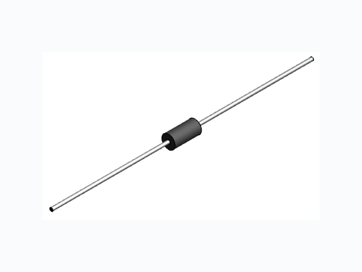
Datasheet - P6KExxA, P6KExxCA - 600 W TVS in DO-15
Document overview
- Manufacturer or author: STMICROELECTRONICS
- PDF pages: 12
Technical content
Features
- Peak pulse power: – 600 W (10/1000 μs) – up to 4 kW (8/20 μs)
- Stand-off voltage range from 5.8 V to 376 V
- Unidirectional and bidirectional types
- Operating Tj max: 175 °C
- High power capability at Tj max.: up to 300 W (10/1000 µs)
- Lead finishing: matte tin plating Complies with the following standards
- UL94, V0
- J-STD-020 MSL level 1
- J-STD-002, JESD 22-B102 E3 and MIL-STD-750, method 2026
- JESD-201 class 2 whisker test
- UL 497B file number: QVGQ2.E136224
- IEC 61000-4-4 level 4: – 4 k V
- IEC 61000-4-2, C = 150 pF, R = 330 Ω exceeds level 4: – 30 kV (air discharge) – 30 kV (contact discharge)
Description
The P6KE TVS series is designed to protect sensitive equipment against electrostatic discharges according to IEC 61000-4-2, MIL STD 883 Method 3015, and electrical overstress such as IEC 61000-4-4 and 5. They are used for surges below 600 W 10/1000 μs. This planar technology makes it compatible with high-end equipment and SMPS where low leakage current and high junction temperature are required to provide reliability and stability over time. DO-15 (JEDEC DO-204AC) K A Product status link P6KE6V8A, P6KE12A, P6KE15A, P6KE18A, P6KE27A, P6KE30A, P6KE33A, P6KE36A, P6KE39A, P6KE47A, P6KE150A, P6KE180A, P6KE200A, P6KE220A, P6KE250A, P6KE300A, P6KE400A, P6KE440A. P6KE6V8CA, P6KE12CA, P6KE15CA, P6KE18CA, P6KE27CA, P6KE30CA, P6KE33CA, P6KE36CA, P6KE39CA, P6KE47CA, P6KE150CA, P6KE180CA, P6KE200CA, P6KE220CA, P6KE250CA, P6KE300CA, P6KE400CA, P6KE440CA.
600 W TVS in DO-15
P6KExxA, P6KExxCA Datasheet DS0681 - Rev 9 - December 2024 For further information contact your local STMicroelectronics sales office.
1 Characteristics
Table 1. Absolute maximum ratings (Tamb = 25 °C) Figure 1. Electrical characteristics - parameter definitions Figure 2. Pulse definition for electrical characteristics
Table 2. Electrical characteristics - parameter values (Tamb = 25 °C, unless otherwise specified)
- To calculate VBR versus Tj : VBR at Tj = VBR at 25 °C x (1 + αT x (Tj - 25))
- To calculate VCL versus Tj : VCL at Tj = VCL at 25 °C x (1 + αT x (Tj - 25))
- To calculate VCL max versus IPPappli: VCL max = VBR max + RD x IPPappli
- Surge capability given for both directions for unidirectional (A type) and bidirectional (CA type) devices
1.1 Characteristics (curves)
Figure 3. Maximum peak power dissipation versus initial Figure 4. Maximum peak pulse power versus exponential Figure 5. Maximum peak pulse current versus clamping Figure 6. Dynamic resistance versus pulse duration Figure 7. Junction capacitance versus reverse applied Figure 8. Junction capacitance versus applied voltage
2 Package information
To meet environmental requirements, ST offers these devices in different grades of ECOPACK packages, depending on their level of environmental compliance. ECOPACK specifications, grade definitions, and product status are available at: www.st.com. ECOPACK is an ST trademark.
2.1 DO-15 package information
Figure 13. DO-15 package outline Table 3. DO-15 package mechanical data
Package information
Figure 19. Tape outline Dimensions are not to scaleUnidirectional components are oriented with red tape on the cathode and white tape on the anode. Bidirectional components have red tape on both sides. Table 4. Tape dimension values
2.2 Reflow profile
Figure 20. ST ECOPACK recommended soldering reflow profile for PCB mounting corresponds to the latest IPC/JEDEC J-STD-020. For wave soldering profile refer to AN5088 chapter 1.5.
- AN5088: Rectifiers thermal management, handling and mounting recommendations. P6KExxA, P6KExxCA
3 Ordering information
Table 5. Ordering information
6000 Reel
- Where xx is nominal value of VBR and A or CA indicates unidirectional or bidirectional version.
Ordering information
Revision history
Table 6. Document revision history 1/ Note 5, figure 7 on page 4, updated from VBR > 220 V to VBR ≥ 200 V. Table 3. Updated footnotes to Table 5. Updated TL temperature in Table 1. 26-Apr-2012 7 Corrected typographical area Table 3. 29-Nov-2022 8 Updated Package information. Minor text changes. 10-Dec-2024 9 Updated Features, Figure 3,Figure 9, and Figure 16.
IMPORTANT NOTICE – READ CAREFULLY STMicroelectronics NV and its subsidiaries (“ST”) reserve the right to make changes, corrections, enhancements, modifications, and improvements to ST products and/or to this document at any time without notice. Purchasers should obtain the latest relevant information on ST products before placing orders. ST products are sold pursuant to ST’s terms and conditions of sale in place at the time of order acknowledgment. Purchasers are solely responsible for the choice, selection, and use of ST products and ST assumes no liability for application assistance or the design of purchasers’ products. No license, express or implied, to any intellectual property right is granted by ST herein. Resale of ST products with provisions different from the information set forth herein shall void any warranty granted by ST for such product. ST and the ST logo are trademarks of ST. For additional information about ST trademarks, refer to www.st.com/trademarks. All other product or service names are the property of their respective owners. Information in this document supersedes and replaces information previously supplied in any prior versions of this document. © 2024 STMicroelectronics – All rights reserved P6KExxA, P6KExxCA DS0681 - Rev 9 page 12/12