
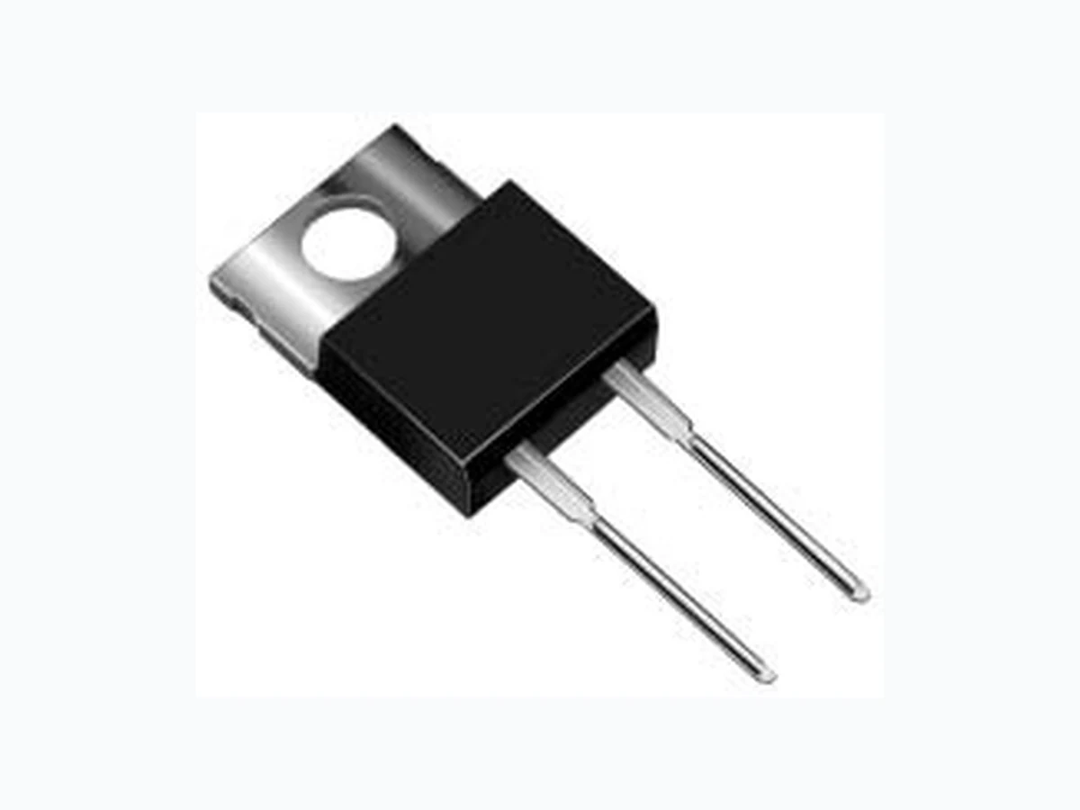
DTV32 VISHAY
Document overview
- Manufacturer or author: Provided By www.digicamel.com(free datasheet download site)
- PDF pages: 4
Technical content
Features
- Glass passivated chip junction High breakdown voltage capability Very fast reverse recovery time IF(AV)1 0 A VRRM 1500 V trr 175 ns tfr 280 ns VF 1.35 V Fast forward recovery time High efficiency, low switching losses Meets MSL level 1, per J-STD-020C Typical Applications For use in high resolution display TV and monitor hor- izontal deflection application Mechanical Data Case: JEDEC TO-220AC, ITO-220AC Terminals: Matte tin plated (E3 Suffix) leads, solder- able per J-STD-002B and MIL-STD-750, Method 2026 Mounting Torque: 10 in-lbs Maximum Epoxy meets UL-94V-0 Flammability rating Maximum Ratings (TC = 25 °C unless otherwise noted) Parameter Test condition Symbol Value Unit Maximum repetitive peak reverse voltage VRRM 1500 V Maximum RMS voltage V RMS 1050 V Maximum DC blocking voltage V DC 1500 V Maximum average forward rectified current (fig. 1) IF(AV) 10 A Peak forward surge current 8.3 ms single half sine-wave superimposed on rated load (JEDEC Method) at TC = 100 °C IFSM 130 A Operating junction and storage temperature range TJ, TSTG -55 to +150 °C RMS Isolation voltage (DTV32F types only) from terminals to heatsink with t = 1.0 second, RH ≤ 30 % V ISOL 4500(1) 3500(2) 1500(3) V
www.vishay.com Document Number 88575 02-Nov-04 VISHAYDTV32 & DTV32F Vishay Semiconductors
Electrical Characteristics
(TC = 25 °C unless otherwise noted) Notes: (1) Clip mounting (on case), where lead does not overlap heatsink with 0.110" offset (2) Clip mounting (on case), where leads do overlap heatsink (3) Screw mounting with 4-40 screw, where washer diameter is ≤ 4.9 mm (0.19") (4) Pulse test: 300 µs pulse width, 2 % duty cycle Thermal Characteristics (TC = 25 °C unless otherwise noted) Parameter Test condition Symbol Value Unit Maximum instantaneous forward voltage(4) IF = 6 A, TJ = 25 °C IF = 6 A, TJ = 125 °C VF 1.5 1.35 V Maximum DC reverse current at VRRM TJ = 25 °C TJ = 125 °C IR 100 1.0 µA mA Maximum reverse recovery time at IF = 1.0 A, di/dt = 50 A/µs, VR = 30 V, Irr = 0.1 IRM trr 175 ns Typical forward recovery time I F = 6 A, di/dt = 48 A/µs, VFR = 3 V t fr 280 ns Peak forward recovery overshoot voltage at IF = 6 A, di/dt = 48 A/µs, TJ = 100 °C Typical Maximum VFP 8 V Parameter Test condition Symbol DTV32 DTV32F Unit Typical thermal resistance from junction to case RθJC 2.0 4.0 °C/W
www.vishay.com Document Number 88575 02-Nov-04 VISHAYDTV32 & DTV32F Vishay Semiconductors Dimensions in Inches and (millimeters) TO-220AC 0.154 (3.91) 0.148 (3.74) DIA. 0.113 (2.87) 0.103 (2.62) 0.185( 4 . 7 0 ) 0.175 (4.44) 0.055 (1.39) 0.045 (1.14) 0.145 (3.68) 0.135 (3.43) 0.350 (8.89) 0.330 (8.38) 0.160 (4.06) 0.140 (3.56) 0.035 (0.90) 0.028 (0.70) 0.205 (5.20) 0.195 (4.95) 0.560 (14.22) 0.530 (13.46) 0.022 (0.56) 0.014 (0.36) 0.110 (2.79) 0.100 (2.54) 12 1.148 (29.16) 1.118 (28.40) 0.105 (2.67) 0.095 (2.41) 0.410 (10.41) 0.625 (15.87) 0.603 (15.32) 0.573 (14.55) PIN 0.415 (10.54) MAX. 0.370 (9.40) 0.360 (9.14) 0.057 (1.45) 0.045(1.14) 0.405 (10.27) 0.383 (9.72) 0.191 (4.85) 0.171 (4.35) 0.600 (15.5) 0.580 (14.5) 0.560 (14.22) 0.530 (13.46) 0.037 (0.94) 0.027 (0.69) 0.140 (3.56) 0.130 (3.30) 0.350 (8.89) 0.330 (8.38) 0.188 (4.77) 0.172 (4.36) 0.110 (2.80) 0.100 (2.54) 0.131 (3.39) 0.122 (3.08) 0.110 (2.80) 0.100 (2.54) 0.022 (0.55) 0.195 (4.95) PIN DIA.DIA. 0.676 (17.2) 0.646 (16.4) ITO-220AC 0.057 (1.45) 0.045(1.14)