


 Download PDF
DCR010503 TI1
Document overview
- PDF pages: 28
Technical content
Page 1
Product
Tools &
Support &
Technical
Sample &
Reference
Folder
Software
Community
Documents
Buy
Design
DCR01 Series, 1-W, 1000-Vrms Isolated, Regulated DC–DC Converter Modules
1 Features
- 1000-Vrms Isolation (Operational)
- UL1950 Recognized Component
- 53 W/in3 (3.3W/cm3) Power Density
- 10-Pin PDIP and 12-Pin SOP Packages
- Device-to-Device Synchronization
- Thermal Protection
- 400-kHz Switching
- 125 FITs at 55ºC
- ±10% Input Range
- Short-Circuit Protected
- 5-V, 12-V, and 24-V Inputs
- 3.3-V and 5-V Outputs
- High Efficiency
2 Applications
- Point-of-Use Power Conversion
- Digital Interface Power
- Ground Loop Elimination
- Power-Supply Noise Reduction
3 Description
The DCR01 family is a series of high-efficiency, inputisolated, output-regulated DC–DC converters. In addition to 1 W nominal, galvanically-isolated output power capability, this range of DC–DCs offer very low output noise, thermal protection, and high accuracy. This combination of features and small size makes the DCR01 series of devices suitable for a wide range of applications, and is an easy-to-use solution in applications requiring signal path isolation.
Device Information(1)
| PART NUMBER | PACKAGE | BODY SIZE (NOM) |
|---|---|---|
| DCR01 | PDIP (10) | 22.86 mm × 6.61 mm |
| SOP (12) | 17.90 mm × 7.50 mm |
(1) For all available packages, see the orderable addendum at the end of the data sheet.
DCR01 Block Diagram
+VS
VREC
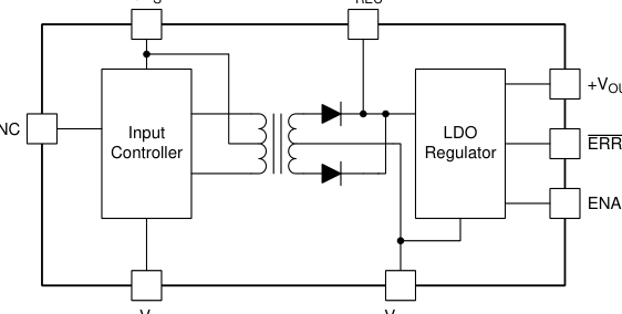
SYNC
ERROR
ENABLE
-VS
-VOUT Copyright © 2016, Texas Instruments Incorporated
An IMPORTANT NOTICE at the end of this data sheet addresses availability, warranty, changes, use in safety-critical applications, intellectual property matters and other important disclaimers. PRODUCTION DATA.
Page 2
Table of Contents
1 Features.................................................................. 1 2 Applications ........................................................... 1 3 Description ............................................................. 1 4 Revision History..................................................... 2 5 Device Comparison Table..................................... 3 6 Pin Configuration and Functions......................... 4 7 Specifications......................................................... 5 7.1 Absolute Maximum Ratings ...................................... 5 7.2 ESD Ratings.............................................................. 5
7.3 Recommended Operating Conditions....................... 5 7.4 Thermal Information.................................................. 5 7.5 Electrical Characteristics........................................... 6 7.6 Typical Characteristics.............................................. 7 8 Detailed Description ............................................ 11 8.1 Overview ................................................................. 11 8.2 Functional Block Diagram ....................................... 11 8.3 Feature Description................................................. 11
4 Revision History
Changes from Revision C (May 2003) to Revision D
8.4 Device Functional Modes........................................ 14 9 Application and Implementation ........................ 15 9.1 Application Information............................................ 15 9.2 Typical Application ................................................. 17 10 Power Supply Recommendations ..................... 18 11 Layout................................................................... 18 11.1 Layout Guidelines ................................................. 18 11.2 Layout Examples................................................... 19 12 Device and Documentation Support ................. 20 12.1 Receiving Notification of Documentation Updates 20
12.2 Related Links ........................................................ 20 12.3 Community Resources.......................................... 20 12.4 Trademarks........................................................... 20 12.5 Electrostatic Discharge Caution............................ 20 12.6 Glossary................................................................ 20 13 Mechanical, Packaging, and Orderable Information ........................................................... 20
Page
- Added Device Information table, Device Comparison table, ESD Ratings table, Thermal Information table, Feature Description section, Device Functional Modes, Application and Implementation section, Power Supply Recommendations section, Layout section, Device and Documentation Support section, and Mechanical, Packaging, and Orderable Information section. ..................................................................................................................... 1
- Removed Package/Ordering Information table, see POA at the end of the data sheet ....................................................... 1
- Added additional graphs to the Typical Characteristics section ............................................................................................ 7
- Added Isolation section to the Feature Description section ................................................................................................ 11
- Added a typical application design to the Application Information section .......................................................................... 15
Page 3
5 Device Comparison Table
at TA = 25°C, +VS = nominal, IO = 10 mA, CIN = 2.2-µF ceramic, CFILTER = 1-µF ceramic, COUT = 0.1-µF ceramic (unless
otherwise noted)
| DEVICE NUMBER (1) | INPUT VOLTAGE VS (V) | OUTPUT VOLTAGE VO (V) | OUTPUT CURRENT (mA) | RIPPLE (2) (mVp-p) | NOISE (3) (mVp-p) | SUPPLY CURRENT (mA) | ||
| IO = 0 mA | IO = 10 mA | IO = 100% LOAD | ||||||
| TYP | TYP | MAX | TYP | TYP | TYP | TYP | TYP | |
| DCR010503P | 5 | 3.3 | 300 | 5 | 35 | 18 | 28 | 335 |
| DCR010503U | 8 | 23 | 24 | 33 | 339 | |||
| DCR010505P | 5 | 200 | 6 | 20 | 25 | 40 | 306 | |
| DCR010505U | 9 | 20 | 25 | 40 | 306 | |||
| DCR011203P | 12 | 3.3 | 390 | 10 | 54 | 13 | 17 | 173 |
| DCR011203U | 300 | 8 | 22 | 13 | 17 | 136 | ||
| DCR011205P | 5 | 200 | 6 | 45 | 13 | 18 | 125 | |
| DCR011205U | 6 | 21 | 14 | 19 | 123 | |||
| DCR012403P | 24 | 3.3 | 390 | 10 | 22 | 17 | 18 | 97 |
| DCR012403U | 300 | 8 | 22 | 15 | 17 | 75 | ||
| DCR012405P | 5 | 200 | 10 | 22 | 15 | 18 | 69 | |
| DCR012405U | 13 | 32 | 15 | 18 | 67 | |||
(1) The last character in the part number denotes the package type; P = PDIP, U = SOP (2) 20-MHz Bandwidth, 50% Load (3) 100-MHz Bandwidth, 50% Load
Page 4
6 Pin Configuration and Functions
NVE Package
DVB Package
10-Pin PDIP
12-Pin SOP
Top View
Top View
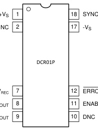
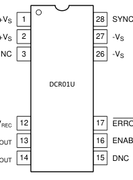
-VOUT
-VOUT
+VOUT
+VOUT
Pin Functions
| PIN | I/O | DESCRIPTION | ||
|---|---|---|---|---|
| NAME | PDIP | SOP | ||
| ENABLE | 11 | 16 | I | Output Voltage Enable |
| ERROR | 12 | 17 | O | Error Flag Active Low |
| DNC | 10 | 15 | — | Do Not Connect |
| NC | 2 | 3 | — | No Connection |
| SYNC | 18 | 28 | I | Synchronization Input |
| –V OUT | 8 | 13 | O | Output Ground |
| +V OUT | 9 | 14 | O | Voltage Output |
| V REC | 7 | 12 | O | Rectified Output |
| –V S | 17 | 26, 27 | I | Input Ground |
| +V S | 1 | 1, 2 | I | Voltage Input |
Page 5
7 Specifications
7.1 Absolute Maximum Ratings
over operating free-air temperature range (unless otherwise noted)(1)(2)
| MIN MAX | UNIT | |||
|---|---|---|---|---|
| Input voltage | 5-V input devices | 7 | V | |
| 12-V input devices | 15 | |||
| 24-V input devices | 29 | |||
| Lead temperature | PDIP package | Surface temperature of device body or pins (maximum 10 s) | 270 | °C |
| Reflow solder temperature | SOP package | Surface temperature of device body or pins | 260 | °C |
| Storage temperature, T stg | –60 125 | °C | ||
(1) Stresses beyond those listed under Absolute Maximum Ratings may cause permanent damage to the device. These are stress ratings only, which do not imply functional operation of the device at these or any other conditions beyond those indicated under Recommended Operating Conditions. Exposure to absolute-maximum-rated conditions for extended periods may affect device reliability. (2) See the package option addendum at the end of the datasheet for additional package information.
7.2 ESD Ratings
| VALUE | UNIT | ||
|---|---|---|---|
| V Electrostatic discharge (ESD) | Human-body model (HBM), per ANSI/ESDA/JEDEC JS-001(1) | ±1000 | V |
| Charged-device model (CDM), per JEDEC specification JESD22-C101(2) | ±250 | ||
(1) JEDEC document JEP155 states that 500-V HBM allows safe manufacturing with a standard ESD control process. (2) JEDEC document JEP157 states that 250-V CDM allows safe manufacturing with a standard ESD control process.
7.3 Recommended Operating Conditions
over operating free-air temperature range (unless otherwise noted)
| MIN NOM MAX | UNIT | ||
|---|---|---|---|
| Input voltage | 5-V input devices | 4.5 5 5.5 | V |
| 12-V input devices | 10.8 12 13.2 | ||
| 24-V input devices | 21.6 24 26.4 | ||
| Operating temperature | –40 85 | °C | |
7.4 Thermal Information
| THERMAL METRIC(1) | DCR01 | UNIT | |
|---|---|---|---|
| NVE (PDIP) | DVB (SOP) | ||
| 10 PINS | 12 PINS | ||
| R Junction-to-ambient thermal resistance θJA | 60 | 60 | °C/W |
| R Junction-to-case (top) thermal resistance θJC(top) | 26 | 26 | °C/W |
| R Junction-to-board thermal resistance θJB | 24 | 24 | °C/W |
| ψ Junction-to-top characterization parameter JT | 7 | 7 | °C/W |
| ψ Junction-to-board characterization parameter JB | 24 | 24 | °C/W |
(1) For more information about traditional and new thermal metrics, see the Semiconductor and IC Package Thermal Metrics application report.
Page 6
7.5 Electrical Characteristics
at TA = 25°C, +VS = nominal, IO = 10 mA, CIN = 2.2-µF ceramic, CFILTER = 1-µF ceramic, COUT = 0.1-µF ceramic (unless otherwise noted)
| PARAMETER | TEST CONDITIONS | MIN TYP MAX | UNIT | |
|---|---|---|---|---|
| OUTPUT | ||||
| Nominal output voltage (+V ) OUT | DCR01xx03 | 3.3 | V | |
| DCR01xx05 | 5 | |||
| Setpoint accuracy | 0.5% 2% | |||
| Output short-circuit protected | Duration | Infinite | ||
| Line regulation | 1 | mV/V | ||
| Over line and load | I = 10 mA to Full Load, Over +V range O S | 1% 2.5% | ||
| Temperature variation | –40°C ≤T ≤+85°C A | 1% | ||
| INPUT | ||||
| Nominal input voltage (+V ) S | DCR0105xx | 5 | V | |
| DCR0112xx | 12 | |||
| DCR0124xx | 24 | |||
| Voltage range | –10% 10% | |||
| Reflected ripple current | 20-MHz Bandwidth, I = 100% Load O | 8 | mAp-p | |
| ISOLATION | ||||
| Isolation | 1-s Flash Test | Voltage | 1 | kVrms |
| dV/dt | 500 | V/s | ||
| Leakage Current | 30 | nA | ||
| Continuous working voltage across isolation barrier | DC | 60 | VDC | |
| AC | 42.5 | VAC | ||
| Barrier capacitance | 25 | pF | ||
| OUTPUT ENABLE CONTROL | ||||
| Logic high input voltage | 2 V REC | V | ||
| Logic high input current | 2 < V < V ENABLE REC | 100 | nA | |
| Logic low input voltage | –0.2 0.5 | V | ||
| Logic low input current | 0 < V < 0.5 ENABLE | 100 | nA | |
| Rectified output, V REC | All 3.3-V Outputs | 3.3 | V | |
| All 5-V Outputs | 5 | |||
| ERROR FLAG | ||||
| Logic high open-collector leakage | V = 5 V ERROR | 10 | µA | |
| Logic low output voltage | Sinking 2 mA | 0.4 | V | |
| THERMAL SHUTDOWN | ||||
| Junction temperature | Temperature Activated | 150 | °C | |
| Temperature Deactivated | 130 | |||
| SYNCHRONIZATION PIN | ||||
| Max external capacitance on SYNC pin | 3 | pF | ||
| Internal oscillator frequency | 720 800 880 | kHz | ||
| External synchronization frequency | 720 880 | kHz | ||
| External synchronization signal high | 2.5 3 | V | ||
| External synchronization signal low | 0 0.4 | V | ||
| TEMPERATURE RANGE | ||||
| Operating | –40 85 | °C | ||
Page 7
7.6 Typical Characteristics
at TA = 25°C, +VS = nominal, IO = 10 mA, CIN = 2.2 µF, CFILTER = 1 µF, COUT = 0.1 µF, (unless otherwise noted)
| 70 85°C 60 50 –40°C (%) 40 Efficiency 25°C 30 20 10 0 0 10 20 30 40 50 60 70 80 90 100 Load (%) DCR010503P, DCR010503U DCR011205P, DCR011205U Figure 1. Efficiency vs Load | 80 +85°C 70 +25°C 60 (%) 50 Effeciency 40 –40°C 30 20 10 0 0 10 20 30 40 50 60 70 80 90 100 Load (%) DCR010505P, DCR010505U DCR011205P, DCR011205U Figure 2. Efficiency vs Load |
| 60 50 40 (%) Efficiency 30 20 10 0 0 10 20 30 40 50 60 70 80 90 100 Load% DCR012403P DCR012403U Figure 3. Efficiency vs Load | 70 60 50 (%) 40 Efficiency 30 20 10 0 0 10 20 30 40 50 60 70 80 90 100 Load (%) DCR010505U DCR011205U Figure 4. Efficiency vs Load |
| 70 60 50 (%) 40 Efficiency 30 20 10 0 0 10 20 30 40 50 60 70 80 90 100 Load (%) DCR012405P DCR012405U Figure 5. Efficiency vs Load | 18 16 14 (mVp-p) 12 10 Voltage 8 6 Ripple 4 2 0 0 20 40 60 80 100 Load (%) All devices except for DCR011203P & DCR012403P 20-MHz Bandwidth Figure 6. Output Voltage Ripple |
Page 8
Typical Characteristics (continued)
at TA = 25°C, +VS = nominal, IO = 10 mA, CIN = 2.2 µF, CFILTER = 1 µF, COUT = 0.1 µF, (unless otherwise noted)
| 30.0 25.0 (mVp-p) 20.0 Voltage 15.0 Ripple 10.0 5.0 0 0 20 40 60 80 100 Load (%) DCR011203P 20-MHz Bandwidth DCR012403P Figure 7. Output Voltage Ripple | 80 70 60 50 (mVp-p) 40 Noise 30 20 10 0 0 20 40 60 80 100 Load (%) All 5-V Input Devices 100-MHz Bandwidth Figure 8. Output Voltage Noise |
| 120.0 100.0 80.0 (mVp-p) 60.0 Noise 40.0 20.0 0 0 20 40 60 80 100 Load (%) DCR011203P 100-MHz Bandwidth Figure 9. Output Voltage Noise | 60.0 50.0 40.0 (mVp-p) 30.0 Noise 20.0 10.0 0 0% 20% 40% 60% 80% 100% Load% DCR011205P 100-MHz Bandwidth Figure 10. Output Voltage Noise |
| All 5-V Output Devices Figure 11. 5-V Output Load Regulation | All 3.3-V output devices except DCR010503P Figure 12. 3.3-V Output Load Regulation |
Page 9
Typical Characteristics (continued)
at TA = 25°C, +VS = nominal, IO = 10 mA, CIN = 2.2 µF, CFILTER = 1 µF, COUT = 0.1 µF, (unless otherwise noted)
| 3.305 85°C 3.3 3.295 3.29 (V) 3.285 OUT 25°C V 3.28 3.275 3.27 –40°C 3.265 0 10 20 30 40 50 60 70 80 90 100 Load (%) DCR010503P Figure 13. 3.3-V Output Load Regulation | 20mA/div 500ns/div 20-MHz Bandwidth Figure 14. Input Current Reflected Ripple |
| 40mA/div 500ns/div 100-MHz Bandwidth Figure 15. Input Current Reflected Ripple | 5mV/div 200ns/div 20-MHz Bandwidth Figure 16. DCR010505P Output Voltage Ripple at 100% Load |
| 20mV/div 200ns/div 100-MHz Bandwidth Figure 17. DCR010505P Output Voltage Noise at 100% Load | 5mV/div 200ns/div 20-MHz Bandwidth Figure 18. DCR010503P Output Voltage Ripple at 100% Load |
Page 10
Typical Characteristics (continued)
at TA = 25°C, +VS = nominal, IO = 10 mA, CIN = 2.2 µF, CFILTER = 1 µF, COUT = 0.1 µF, (unless otherwise noted)
| Load Current 20mV/div Output Voltage 200ns/div 100-MHz Bandwidth Figure 19. DCR010503P Output Voltage Noise at 100% Load | Load Current Changing 325mA 30mA to Output Voltage 200mV/div 10µs/div Figure 20. DCR010503P Load Transient Response |
| Load Current Changing 300mA 150mA to 200mV/div Output Voltage 10µs/div Figure 21. DCR010503P Load Transient Response | Load Current Changing 200mA 20mA to Output Voltage 200mV/div 10µs/div Figure 22. DCR010505P Load Transient Response |
| Load Current Changing 200mA 100mA to Output Voltage 200mV/div 10µs/div Figure 23. DCR010505P Load Transient Response | |
Page 11
8 Detailed Description
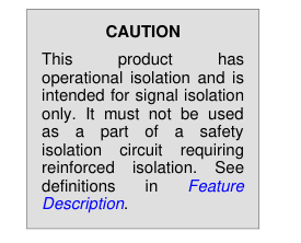
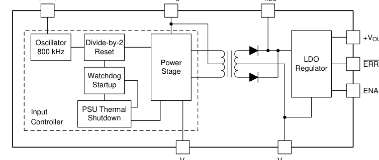
8.1 Overview The DCR01 series of power modules offer isolation from a regulated power supply operating from a choice of input voltages. The DCR01s provide a regulated 3.3-V or 5-V output voltage at a nominal output power of 1 W or above. The DCR01 devices include a low dropout linear regulator internal to the device to achieve a wellregulated output voltage. The DCR01 devices are specified for operational isolation only. The circuit design uses an advanced BiCMOS/DMOS process.
8.2 Functional Block Diagram
SYNC
+VS
VREC
ERROR
ENABLE
-VS
-VOUT
Copyright © 2016, Texas Instruments Incorporated
8.3 Feature Description
8.3.1 Isolation Underwriters Laboratories, UL™, defines several classes of isolation that are used in modern power supplies. Safety extra low voltage (SELV) is defined by UL (UL1950 E199929) as a secondary circuit which is so designated and protected that under normal and single fault conditions the voltage between any two accessible parts, or between an accessible part and the equipment earthing terminal for operational isolation does not exceed steady state 42.4 VRMS or 60 VDC peak.
8.3.1.1 Operation or Functional Isolation The type of isolation used in the DCR01 products is referred to as operational or functional isolation. Insulated wire used in the construction of the transformer acts as the primary isolation barrier. A high-potential (hipot), onesecond duration test (dielectric voltage, withstand test) is a production test used to verify that the isolation barrier is functioning. Products with operational isolation must never be used as an element in a safety-isolation system.
8.3.1.2 Basic or Enhanced Isolation Basic or enhanced isolation is defined by specified creepage and clearance limits between the primary and secondary circuits of the power supply. Basic isolation is the use of an isolation barrier in addition to the insulated wire in the construction of the transformer. Input and output circuits must also be physically separated by specified distances.
Page 12
Feature Description (continued)
NOTE
The DCR01 products DO NOT provide basic or enhanced isolation.
8.3.1.3 Working Voltage For a device with operational isolation, the continuous working voltage that can be applied across the device in normal operation must be less than 42.4 VRMS or 60 VDC, (SELV limits).

If the device is expected to function correctly with more than 42.4 VRMS or 60 VDC applied continuously across the isolation barrier, then the circuitry on both sides of the barrier must be regarded as operating at an unsafe voltage, and further isolation or insulation systems must form a barrier between these circuits and any useraccessible circuitry according to safety standard requirements.
8.3.1.4 Isolation Voltage Rating The terms Hipot test, flash-tested, withstand voltage, proof voltage, dielectric withstand voltage, and isolation test voltage are all terms that relate to the same thing; a test voltage applied for a specified time across a component designed to provide electrical isolation to verify the integrity of that isolation. TI’s DCR01 series of DC-DC converters are all 100% production tested at 1 kVAC for one second.
8.3.1.5 Repeated High-Voltage Isolation Testing Repeated high-voltage isolation testing of a barrier component can degrade the isolation capability, depending on materials, construction, and environment. The DCV01 series of DC–DC converters have toroidal, enameled, wire isolation transformers with no additional insulation between the primary and secondary windings. While a device can be expected to withstand several times the stated test voltage, the isolation capability depends on the wire insulation. Any material, including this enamel (typically polyurethane), is susceptible to eventual chemical degradation when subject to very-high applied voltages. Therefore, strictly limit the number of high-voltage tests
and repeated high-voltage isolation testing. However, if it is absolutely required, reduce the voltage by 20% from specified test voltage with a duration limit of one second per test.
8.3.2 Power Stage The DCR01 series of devices use a push-pull, center-tapped topology. The DCV01 devices switch at 400 kHz (divide-by-2 from an 800-kHz oscillator).
8.3.3 Rectification The transformer’s output is full wave rectified and filtered by the external 1-μF ceramic capacitor connected to VREC.
8.3.4 Regulator The internal low dropout linear regulator provides a well-regulated output voltage throughout the operating range of the device.
8.3.5 Oscillator and Watchdog The onboard, 800-kHz oscillator generates the switching frequency through a divide-by-2 circuit. The oscillator can be synchronized to other DCR01 device circuits or an external source, and is used to minimize system noise.
Page 13
Feature Description (continued) A watchdog circuit monitors the operation of the oscillator circuit. The oscillator can be disabled by pulling the SYNC pin low. When the SYNC pin goes low, the output pins transition into tri-state mode, which occurs within 2 μs.
8.3.6 ERROR Flag The DCR01 has an ERROR pin which provides a power good flag, as long as the internal regulator is in regulation. If the ERROR output is required, place a 10-kΩ resistor between the ERROR pin and the output voltage.
8.3.7 Synchronization When more than one DC–DC converter is switching in an application, beat frequencies and other electrical interference can be generated. This interference occurs because of the small variations in switching frequencies between the DC–DC converters. The DCR01 series of devices overcome this interference by allowing devices to be synchronized to one another. Synchronize up to eight devices by connecting the SYNC pins of each device, taking care to minimize the capacitance of tracking. Stray capacitance (greater than 3 pF) reduces the switching frequency, or can sometimes stop the oscillator circuit. The maximum recommended voltage applied to the SYNC pin is 3 V.
For an application that uses more than eight synchronized devices use an external device to drive the SYNC pins. The application report External Synchronization of the DCP01/02 Series of DC/DC Converters describes this configuration.
NOTE
During the start-up period, all synchronized devices draw maximum current from the input simultaneously. If the input voltage falls below approximately 4 V, the devices may not start up. A ceramic capacitor should be connected close to each device's input pin. Use a 2.2-μF capacitor for 5-V input devices, and a 0.47-μF capacitor for the 12-V and 24-V devices.
8.3.8 Construction The basic construction of the DCR01 series of devices is the same as standard integrated circuits. The molded package contains no substrate. The DCV01 series of devices are constructed using an IC, low dropout linear regulator, rectifier diodes, and a wound magnetic toroid on a leadframe. Because the package contains no solder, the devices do not require any special printed-circuit board (PCB) assembly processing. This architecture results in an isolated DC–DC converter with inherently high reliability.
8.3.9 Thermal Considerations Due to the high power density of this device, it is advisable to provide ground planes on the input and output rails. The output regulator is mounted on a copper leadframe, and a ground plane serves as an efficient heatsink.
8.3.10 Decoupling – Ripple Reduction Due to the very low forward resistance of the DMOS switching transistors, high current demands are placed upon the input supply for a short time. By using a good quality low Equivalent Series Resistance (ESR) capacitor of 2.2 μF (minimum) for the 5-V input devices and a 0.47-μF capacitor for the 12-V and 24-V devices, placed close to the IC supply input pins, the effects on the power supply can be minimized. The high switching frequency of 400 kHz allows relatively small values of capacitors to be used for filtering the rectified output voltage. A good-quality, low-ESR, 1-μF ceramic capacitor placed close to the VREC pin and
output ground is required and reduces the ripple. The output at VREC is full wave rectified and produces a ripple of 800 kHz. TI recommends that a 0.1-μF, low-ESR, ceramic capacitor is connected close to the output pin and ground to reduce noise on the output. The capacitor values listed are minimum values. If lower ripple is required, the filter capacitor should be increased in value to 2.2 μF.
Page 14
Feature Description (continued) As with all switching power supplies, the best performance is obtained with low ESR,ceramic capacitors connected close to the device pins. If low ESR, ceramic capacitors are not used, the ESR generates a voltage drop when the capacitor is supplying the load power. Often a larger capacitor is chosen for this purpose, when a low ESR, smaller capacitor would perform as well.
NOTE
TI does not recommend that the DCR01 be fitted using an IC socket, as this degrades performance.
8.4 Device Functional Modes
8.4.1 Device Disable and Enable Each of the DCR01 series devices can be disabled or enabled by driving the SYNC pin using an open-drain CMOS gate. If the SYNC pin is pulled low, the DCR01 becomes disabled. The disable time depends upon the external loading. The internal disable function is implemented in 2 μs. Removal of the pulldown causes the DCR01 to be enabled. Capacitive loading on the SYNC pin must be minimized (≤ 3 pF) to prevent a reduction in the oscillator frequency. The application report External Synchronization of the DCP01/02 Series of DC/DC Converters describes disable and enable control circuitry. This document contains information on how to null the effects of
additional capacitance on the SYNC pin. The oscillator’s frequency can be measured at VREC, as this is the fundamental frequency of the ripple component.
8.4.2 Regulated Output Disable and Enable The regulated output of the DCR01 can be disabled by pulling the ENABLE pin LOW. Disabling the output voltage this way still produces a voltage on the VREC pin. When using the ENABLE control, TI recommends placing a 10-kΩ resistor between the VREC and ENABLE pins. The ENABLE pin only controls the internal linear regulator. If disabling the regulated output is not required, pull the ENABLE pin HIGH by shorting it directly to the VREC pin. This enables the regulated output voltage, thus allowing the output to be controlled from the isolated side.
Page 15
9 Application and Implementation
NOTE
Information in the following applications sections is not part of the TI component specification, and TI does not warrant its accuracy or completeness. TI’s customers are responsible for determining suitability of components for their purposes. Customers should validate and test their design implementation to confirm system functionality.
9.1 Application Information
9.1.1 DCR01 Single Voltage Output The DCR01 can be used to provide a single voltage output by connecting it as shown in Figure 24. The ERROR output signal will be pulled up to the value of VOUT . The value of RERR will depend on the loading on the ERROR line; however, the total load on the ERROR line must not exceed the value given in Electrical Characteristics. The output may be permanently enabled by connecting the ENABLE pin to the VREC pin. The DCR01 may be enabled remotely by connecting the ENABLE pin to VREC through a pullup resistor (REN); the value of this resistor is not critical for the DCR01 as only a small current flows. The switch SW1 can be used to pull the ENABLE pin
LOW, thus disabling the output. The switching devices can be a bipolar transistor, FET, or a mechanical device; the main load that it sees is REN.
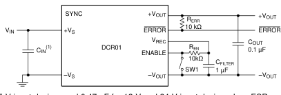
(1) CIN = 2.2 μF for 5-V input devices and 0.47 μF for 12-V and 24-V input devices. Low ESR, ceramic capacitors are required.
Figure 24. DCR01 Single Output Voltage
Page 16
Application Information (continued) 9.1.2 Generating Two Positive Output Voltages Two DCR01s can be used to create output voltages of +3.3 V and +5 V, as shown in Figure 25. The two DCR01s are connected in self-synchronization, thus locking the oscillators of both devices to a single frequency. The ERROR and ENABLE facilities may be used in a similar configuration for a single DCR01. The filter capacitors connected to the VREC pins (CFILTER) must be kept separate from each other and connected in close proximity to their respective DCR01.
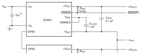
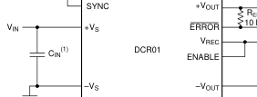
| RERR 10 k | ||
| CFILTER 1 µF | COUT 0.1 µF | |
ERROR2
(1) CIN = 2.2 μF for 5-V input devices and 0.47 μF for 12-V and 24-V input devices. Low ESR, ceramic capacitors are required.
Figure 25. Two Positive Voltages from Self-Synchronized DCR01s
9.1.3 Generation of Dual Polarity Voltages from Two Self-Synchronized DCR01s Two DCR01s can be configured to produce a dual polarity supply (that is, ±5 V); the circuit must be connected as shown in Figure 26. It must be observed that both devices are producing a positive regulated output; therefore the ERROR, ENABLE, and VREC are all relative to that particular device's –VOUT pin and must not be directly connected together, or in the case of the negative output device, connected to the common 0-V output.
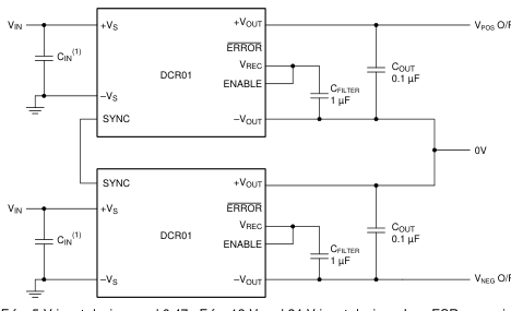
(1) CIN = 2.2 μF for 5-V input devices and 0.47 μF for 12-V and 24-V input devices. Low ESR, ceramic capacitors are required.
Figure 26. Dual Polarity Voltage Generation
Page 17
9.2 Typical Application
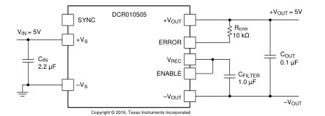
Figure 27. DCR01 Typical Schematic
9.2.1 Design Requirements For this design example, use the parameters listed in Table 1 and follow the design procedure.
Table 1. Design Example Parameters
| DESIGN PARAMETER | VALUE |
|---|---|
| Input Voltage V IN | 5 V typical |
| Output Voltage V OUT | 5 V regulated |
| Output Current Rating | 200 mA |
| Isolation | 1000-V operational |
9.2.2 Detailed Design Procedure
9.2.2.1 Input Capacitor For this design, a 2.2-μF, ceramic capacitor is required for the input decoupling capacitor.
9.2.2.2 Output Capacitor For this design, a 0.1-μF, ceramic capacitor is required for between +VOUT and –VOUT.
9.2.2.3 Filter Capacitor A high-quality, low-ESR, 1-μF, ceramic capacitor placed close to the VREC pin and output ground is required to reduce output voltage ripple.
9.2.2.4 ERROR Flag Place a 10-kΩ resistor between the ERROR pin and the output voltage to provide a power good signal when the internal regulator is in regulation.
Page 18
9.2.3 Application Curves
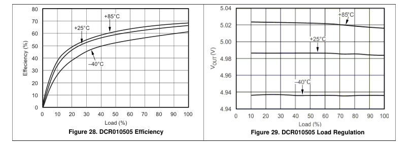
10 Power Supply Recommendations
The DCR01 is a switching power supply, and as such can place high peak current demands on the input supply. To avoid the supply falling momentarily during the fast switching pulses, ground and power planes must be used to connect the power to the input of DCR01. If this connection is not possible, then the supplies must be connected in a star formation with the traces made as wide as possible.
11 Layout
11.1 Layout Guidelines Carefully consider the layout of the PCB in order for the best results to be obtained. Input and output power and ground planes provide a low-impedance path for the input and output power. For the output, the positive and negative voltage outputs conduct through wide traces to minimize losses. A good-quality, low-ESR, ceramic capacitor placed as close as practical across the input reduces reflected ripple and ensure a smooth start-up. A good-quality, low-ESR, ceramic capacitor placed as close as practical across the rectifier output terminal and output ground gives the best ripple and noise performance. The location of the decoupling capacitors in close proximity to their respective pins ensures low losses due to the
effects of stray inductance, thus improving the ripple performance. This location is of particular importance to the input decoupling capacitor, because this capacitor supplies the transient current associated with the fast switching waveforms of the power drive circuits. If the SYNC pin is being used, the tracking between device SYNC pins must be short to avoid stray capacitance. Never connect a capacitor to the SYNC pin. If the SYNC pin is not being used it is advisable to place a guard ring (connected to input ground) around this pin to avoid any noise pick-up. Ensure that no other trace is in close proximity to this trace SYNC trace to decrease the stray capacitance on this pin. The stray capacitance affects
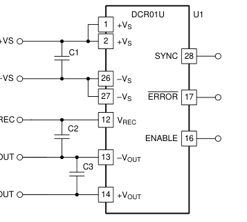
the performance of the oscillator. Figure 30 shows a schematic for a single DCR01, SOP package device. Figure 31 and Figure 32 show a typical layout for the SOP package DCR01 device. The layout shows proper placement of capacitors and power planes.
Page 19
11.2 Layout Examples
VREC
-VOUT
+VOUT
Figure 30. DCR01 PCB Schematic, U Package
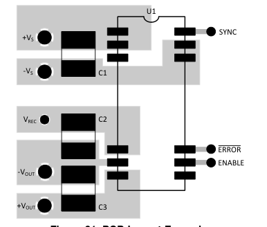
Figure 31. PCB Layout Example, Component-Side View
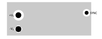
| V REC E E -V OUT +V OUT | |
| RROR NABL |
Figure 32. PCB Layout Example, Non-Component-Side View
Page 20
12 Device and Documentation Support
12.1 Receiving Notification of Documentation Updates
To receive notification of documentation updates, navigate to the device product folder on ti.com. In the upper
right corner, click on Alert me to register and receive a weekly digest of any product information that has
changed. For change details, review the revision history included in any revised document.
12.2 Related Links
The table below lists quick access links. Categories include technical documents, support and community
resources, tools and software, and quick access to sample or buy.
Table 2. Related Links
| PARTS | PRODUCT FOLDER | SAMPLE & BUY | TECHNICAL DOCUMENTS | TOOLS & SOFTWARE | SUPPORT & COMMUNITY |
|---|---|---|---|---|---|
| DCR010503 | Click here | Click here | Click here | Click here | Click here |
| DCR012405 | Click here | Click here | Click here | Click here | Click here |
| DCR010505 | Click here | Click here | Click here | Click here | Click here |
| DCR011203 | Click here | Click here | Click here | Click here | Click here |
| DCR011205 | Click here | Click here | Click here | Click here | Click here |
| DCR012403 | Click here | Click here | Click here | Click here | Click here |
12.3 Community Resources
The following links connect to TI community resources. Linked contents are provided "AS IS" by the respective
contributors. They do not constitute TI specifications and do not necessarily reflect TI's views; see TI's Terms of
Use.
TI E2E™Online Community TI's Engineer-to-Engineer (E2E) Community. Created to foster collaboration
among engineers. At e2e.ti.com, you can ask questions, share knowledge, explore ideas and help
solve problems with fellow engineers.
Design Support TI's Design Support Quickly find helpful E2E forums along with design support tools and
contact information for technical support.
12.4 Trademarks
E2E is a trademark of Texas Instruments.
Underwriters Laboratories, UL are trademarks of UL LLC.
All other trademarks are the property of their respective owners.
12.5 Electrostatic Discharge Caution
This integrated circuit can be damaged by ESD. Texas Instruments recommends that all integrated circuits be handled with appropriate precautions. Failure to observe proper handling and installation procedures can cause damage. ESD damage can range from subtle performance degradation to complete device failure. Precision integrated circuits may be more susceptible to damage because very small parametric changes could cause the device not to meet its published specifications.
12.6 Glossary
SLYZ022 — TI Glossary.
This glossary lists and explains terms, acronyms, and definitions.
13 Mechanical, Packaging, and Orderable Information
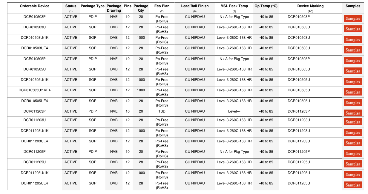
The following pages include mechanical, packaging, and orderable information. This information is the most
current data available for the designated devices. This data is subject to change without notice and revision of
this document. For browser-based versions of this data sheet, refer to the left-hand navigation.
Page 21

PACKAGE OPTION ADDENDUM
28-Jun-2016
PACKAGING INFORMATION
Addendum-Page 1
Page 22

PACKAGE OPTION ADDENDUM
28-Jun-2016
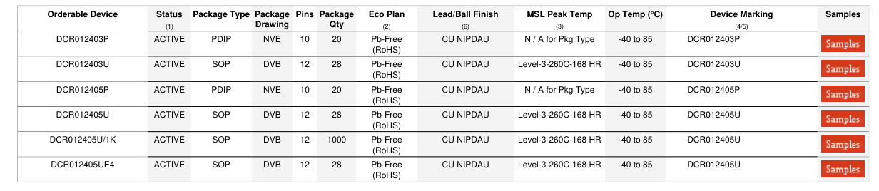
(1) The marketing status values are defined as follows: ACTIVE: Product device recommended for new designs. LIFEBUY: TI has announced that the device will be discontinued, and a lifetime-buy period is in effect. NRND: Not recommended for new designs. Device is in production to support existing customers, but TI does not recommend using this part in a new design. PREVIEW: Device has been announced but is not in production. Samples may or may not be available. OBSOLETE: TI has discontinued the production of the device.
(2) Eco Plan - The planned eco-friendly classification: Pb-Free (RoHS), Pb-Free (RoHS Exempt), or Green (RoHS & no Sb/Br) - please check http://www.ti.com/productcontent for the latest availability information and additional product content details. TBD: The Pb-Free/Green conversion plan has not been defined. Pb-Free (RoHS): TI's terms "Lead-Free" or "Pb-Free" mean semiconductor products that are compatible with the current RoHS requirements for all 6 substances, including the requirement that lead not exceed 0.1% by weight in homogeneous materials. Where designed to be soldered at high temperatures, TI Pb-Free products are suitable for use in specified lead-free processes.
Pb-Free (RoHS Exempt): This component has a RoHS exemption for either 1) lead-based flip-chip solder bumps used between the die and package, or 2) lead-based die adhesive used between the die and leadframe. The component is otherwise considered Pb-Free (RoHS compatible) as defined above. Green (RoHS & no Sb/Br): TI defines "Green" to mean Pb-Free (RoHS compatible), and free of Bromine (Br) and Antimony (Sb) based flame retardants (Br or Sb do not exceed 0.1% by weight in homogeneous material)
(3) MSL, Peak Temp. - The Moisture Sensitivity Level rating according to the JEDEC industry standard classifications, and peak solder temperature.
(4) There may be additional marking, which relates to the logo, the lot trace code information, or the environmental category on the device.
(5) Multiple Device Markings will be inside parentheses. Only one Device Marking contained in parentheses and separated by a "~" will appear on a device. If a line is indented then it is a continuation of the previous line and the two combined represent the entire Device Marking for that device.
Addendum-Page 2
Page 23

PACKAGE OPTION ADDENDUM
28-Jun-2016
(6) Lead/Ball Finish - Orderable Devices may have multiple material finish options. Finish options are separated by a vertical ruled line. Lead/Ball Finish values may wrap to two lines if the finish value exceeds the maximum column width.
Important Information and Disclaimer:The information provided on this page represents TI's knowledge and belief as of the date that it is provided. TI bases its knowledge and belief on information provided by third parties, and makes no representation or warranty as to the accuracy of such information. Efforts are underway to better integrate information from third parties. TI has taken and continues to take reasonable steps to provide representative and accurate information but may not have conducted destructive testing or chemical analysis on incoming materials and chemicals. TI and TI suppliers consider certain information to be proprietary, and thus CAS numbers and other limited information may not be available for release.
In no event shall TI's liability arising out of such information exceed the total purchase price of the TI part(s) at issue in this document sold by TI to Customer on an annual basis.
Addendum-Page 3
Page 24
MECHANICAL DATA
MPDI055 – APRIL 2001
NVE (R-PDIP-T10/18)
PLASTIC DUAL-IN-LINE
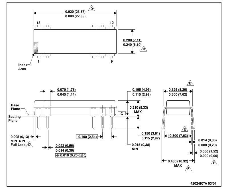
NOTES: A. All linear dimensions are in inches (millimeters). B. This drawing is subject to change without notice. C. Falls within JEDEC MS-001-AC with the exception of lead count. D. Dimensions do not include mold flash or protrusions. Mold flash or protrusions shall not exceed 0.010 (0,25). E. Dimensions measured with the leads constrained to be perpendicular to Datum C. F. Dimensions are measured at the lead tips with the leads unconstrained. G. A visual index feature must be located within the cross-hatched area.
POST OFFICE BOX 655303 • DALLAS, TEXAS 75265
Page 25
PACKAGE OUTLINE
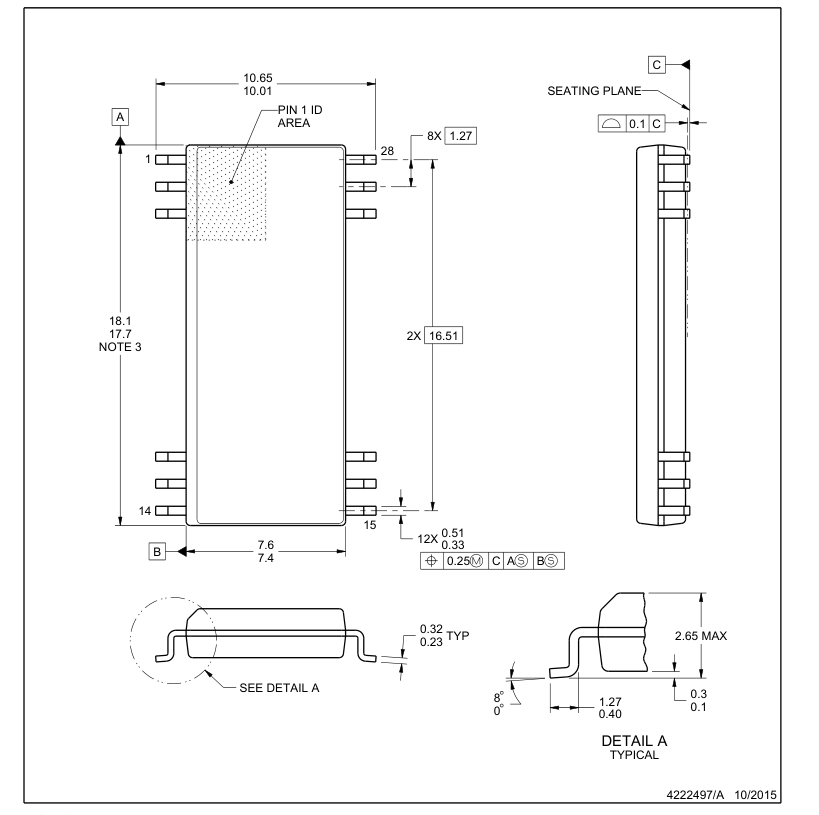
DVB0012A
SOP - 2.65 mm max height
PLASTIC SMALL OUTLINE
NOTES:
- All linear dimensions are in millimeters. Dimensions in parenthesis are for reference only. Dimensioning and tolerancing per ASME Y14.5M. 2. This drawing is subject to change without notice. 3. This dimension does not include mold flash, protrusions, or gate burrs. Mold flash, protrusions, or gate burrs shall not exceed 0.15 mm per side. 4. Reference JEDEC registration MS-013.
Page 26
EXAMPLE BOARD LAYOUT
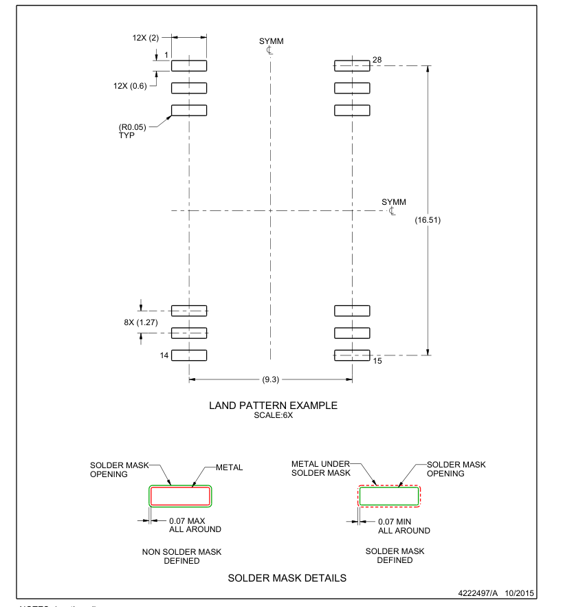
DVB0012A
SOP - 2.65 mm max height
PLASTIC SMALL OUTLINE
NOTES: (continued)
- Publication IPC-7351 may have alternate designs. 6. Solder mask tolerances between and around signal pads can vary based on board fabrication site.
Page 27
EXAMPLE STENCIL DESIGN
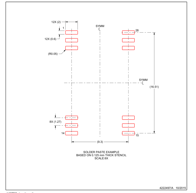
DVB0012A
SOP - 2.65 mm max height
PLASTIC SMALL OUTLINE
NOTES: (continued)
- Laser cutting apertures with trapezoidal walls and rounded corners may offer better paste release. IPC-7525 may have alternate design recommendations. 8. Board assembly site may have different recommendations for stencil design.
Page 28
IMPORTANT NOTICE
Texas Instruments Incorporated and its subsidiaries (TI) reserve the right to make corrections, enhancements, improvements and other changes to its semiconductor products and services per JESD46, latest issue, and to discontinue any product or service per JESD48, latest issue. Buyers should obtain the latest relevant information before placing orders and should verify that such information is current and complete. All semiconductor products (also referred to herein as “components”) are sold subject to TI’s terms and conditions of sale supplied at the time of order acknowledgment. TI warrants performance of its components to the specifications applicable at the time of sale, in accordance with the warranty in TI’s terms
and conditions of sale of semiconductor products. Testing and other quality control techniques are used to the extent TI deems necessary to support this warranty. Except where mandated by applicable law, testing of all parameters of each component is not necessarily performed. TI assumes no liability for applications assistance or the design of Buyers’ products. Buyers are responsible for their products and applications using TI components. To minimize the risks associated with Buyers’ products and applications, Buyers should provide adequate design and operating safeguards. TI does not warrant or represent that any license, either express or implied, is granted under any patent right, copyright, mask work right, or
other intellectual property right relating to any combination, machine, or process in which TI components or services are used. Information published by TI regarding third-party products or services does not constitute a license to use such products or services or a warranty or endorsement thereof. Use of such information may require a license from a third party under the patents or other intellectual property of the third party, or a license from TI under the patents or other intellectual property of TI. Reproduction of significant portions of TI information in TI data books or data sheets is permissible only if reproduction is without alteration
and is accompanied by all associated warranties, conditions, limitations, and notices. TI is not responsible or liable for such altered documentation. Information of third parties may be subject to additional restrictions. Resale of TI components or services with statements different from or beyond the parameters stated by TI for that component or service voids all express and any implied warranties for the associated TI component or service and is an unfair and deceptive business practice. TI is not responsible or liable for any such statements. Buyer acknowledges and agrees that it is solely responsible for compliance with all legal, regulatory and safety-related requirements
concerning its products, and any use of TI components in its applications, notwithstanding any applications-related information or support that may be provided by TI. Buyer represents and agrees that it has all the necessary expertise to create and implement safeguards which anticipate dangerous consequences of failures, monitor failures and their consequences, lessen the likelihood of failures that might cause harm and take appropriate remedial actions. Buyer will fully indemnify TI and its representatives against any damages arising out of the use of any TI components in safety-critical applications. In some cases, TI components may be promoted specifically to facilitate safety-related applications. With such components, TI’s goal is to
help enable customers to design and create their own end-product solutions that meet applicable functional safety standards and requirements. Nonetheless, such components are subject to these terms. No TI components are authorized for use in FDA Class III (or similar life-critical medical equipment) unless authorized officers of the parties have executed a special agreement specifically governing such use. Only those TI components which TI has specifically designated as military grade or “enhanced plastic” are designed and intended for use in military/aerospace applications or environments. Buyer acknowledges and agrees that any military or aerospace use of TI components
which have not been so designated is solely at the Buyer's risk, and that Buyer is solely responsible for compliance with all legal and regulatory requirements in connection with such use. TI has specifically designated certain components as meeting ISO/TS16949 requirements, mainly for automotive use. In any case of use of non-designated products, TI will not be responsible for any failure to meet ISO/TS16949.
Products
Applications
Audio
www.ti.com/audio
Automotive and Transportation
Amplifiers
amplifier.ti.com
Communications and Telecom
Data Converters
dataconverter.ti.com
Computers and Peripherals
DLP® Products
www.dlp.com
Consumer Electronics
DSP
dsp.ti.com
Energy and Lighting
Clocks and Timers
www.ti.com/clocks
Industrial
Interface
interface.ti.com
Medical
Logic
logic.ti.com
Security
Power Mgmt
power.ti.com
Space, Avionics and Defense
Microcontrollers
microcontroller.ti.com
Video and Imaging
RFID
www.ti-rfid.com
OMAP Applications Processors
www.ti.com/omap
TI E2E Community
Wireless Connectivity
www.ti.com/wirelessconnectivity
www.ti.com/automotive www.ti.com/communications www.ti.com/computers www.ti.com/consumer-apps www.ti.com/energy www.ti.com/industrial www.ti.com/medical www.ti.com/security www.ti.com/space-avionics-defense www.ti.com/video
e2e.ti.com
Mailing Address: Texas Instruments, Post Office Box 655303, Dallas, Texas 75265
Copyright © 2016, Texas Instruments Incorporated