

 Download PDF
6406 TUOFENG
Document overview
- Manufacturer or author: Provided By digicamel.com
- PDF pages: 7
Technical content
V DS I D (at V GS R DS(ON) (at V GS Ω R DS(ON) (at V GS Ω Application 100% UIS Tested 100% R g Tested Symbol Units V DS V V GS V MaximumParameter Absolute Maximum Ratings T A =25°C unless otherwise noted =30V
- Latest Trench Power LV technology
- Very Low R DS(on) at 4.5V GS
- Low Gate Charge
- High Current Capability
- RoHS and Halogen-Free Compliant
- DC/DC Converters in Computing, Servers, and POL
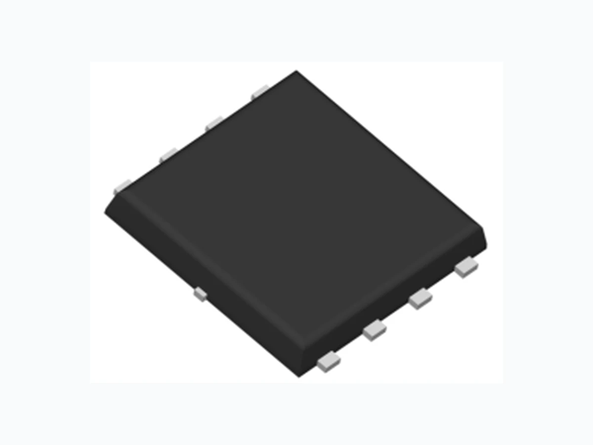
- Isolated DC/DC Converters in Telecom and Industrial Drain-Source Voltage 30 ±20 Gate-Source Voltage G D S Top View Pin 1 V GS V I DM I AS A E AS mJ T J , T STG Symbol Units t ≤ 10s °C/W Steady-State °C/W Steady-State R θJC °C/W Junction and Storage Temperature Range -55 to 150 Power Dissipation B P D Power Dissipation A 180 Avalanche energy L=0.1mH C ±20 Gate-Source Voltage T A =25°C I DSM 280Pulsed Drain Current C AT A =70°C Avalanche Current C Continuous Drain Current G I D 140T C =25°C Continuous Drain Current A W 110 T A =25°C P DSM WT C =25°C 2.3 Thermal Characteristics Maximum Junction-to-Ambient A R θJA Maximum Junction-to-Case Maximum Junction-to-Ambient A D 0.85 1.1 Parameter Typ Max PIN1 Top View Bottom View SHENZHENTUOFENGSEMICONDUCTORTECHNOLOGYCO.,LTD N-Channel Enhancement Mode Power MOSFET www.sztuofeng.com Feb,2018 V1.01 General Features =10V)=140A =10V) 2.5m =4.5V) 3.5m EquivalentCircuit Y :year code W :week code PDFN5X6-8L 6406 TFCYWP S S S G DDD D
V DS =30V, V GS =0V 1 I GSS 10 uA V GS(th) Gate Threshold Voltage 1.3 1.8 2.4 V 2.1 Ω g FS 130 S V SD 0.67 1 V I S 140 C iss 4300 5200 pF C oss 720 pF C rss 420 pF R g 1 2 3 Ω Q g (10V) 70 100 nC Q g (4.5V) 33 nC Q gs 10 nC Q gd 15 nC t D(on) 10 ns t r 6.5 ns t D(off) 75 ns t f 18 ns t rr 30 ns SWITCHING PARAMETERS Maximum Body-Diode Continuous Current G Input Capacitance Output Capacitance Turn-On DelayTime DYNAMIC PARAMETERS Gate resistance V GS =0V, V DS =0V, f=1MHz V GS =10V, V DS =15V, R L =0.75Ω , R GEN =3Ω Reverse Transfer Capacitance V GS =0V, V DS =15V, f=1MHz µ Turn-Off DelayTime V GS =10V, V DS =15V, I D =20A Gate Source Charge Gate Drain Charge Total Gate Charge Body Diode Reverse Recovery Time Turn-Off Fall Time Total Gate Charge I F =20A, dI/dt=500A/µs Turn-On Rise Time Static Drain-Source On-Resistance Diode Forward Voltage V DS =5V, I D =20A V GS =4.5V, I D =20A Forward Transconductance I S =1A,V GS =0V Electrical Characteristics (T J =25°C unless otherwise noted) STATIC PARAMETERS Parameter Conditions mΩ I DSS Drain-Source Breakdown Voltage I D =250µA, V GS =0V µAZero Gate Voltage Drain Current Gate-Body leakage current V DS GS I D =250µA V DS =0V, V GS = ±16V V GS =10V, I D =20AR DS(ON) Q rr 15 nCBody Diode Reverse Recovery Charge I F =20A, dI/dt=500A/ µ s A. The value of RθJA is measured with the device mounted on 1in2 FR-4 board with 2oz. Copper, in a still air environment with TA =25°C. The Power dissipation PDSM is based on R θJA and the maximum allowed junction temperature of 150°C. The value in any given application depends on the user's specific board design, and the maximum temperature of 150°C may be used if the PCB allows it. B. The power dissipation PD is based on TJ(MAX)=150°C, using junction-to-case thermal resistance, and is more useful in setting the upper dissipation limit for cases where additional heatsinking is used. C. Repetitive rating, pulse width limited by junction temperature TJ(MAX)=150°C. Ratings are based on low frequency and duty cycles to keep initial TJ =25°C. D. The RθJA is the sum of the thermal impedence from junction to case RθJC and case to ambient. E. The static characteristics in Figures 1 to 6 are obtained using <300µs pulses, duty cycle 0.5% max. F. These curves are based on the junction-to-case thermal impedence which is measured with the device mounted to a large heatsink, assuming a maximum junction temperature of TJ(MAX)=150°C. The SOA curve provides a single pulse rating. G. The maximum current rating is package limited. H. These tests are performed with the device mounted on 1 in2 FR-4 board with 2oz. Copper, in a still air environment with TA=25°C. 6406 SHENZHENTUOFENGSEMICONDUCTORTECHNOLOGYCO.,LTD N-Channel Enhancement Mode Power MOSFET www.sztuofeng.com Feb,2018 V1.02 2.5 m3.52.6 A
Gate Charge Test Circuit & Waveform VDC DUT Vdd Vgs Vds Vgs RL Rg Vgs Vds 10% 90% Resistive Switching Test Circuit & Waveforms t t r d(on) t on t d(off) t f t off Id L Vds BV Unclamped Inductive Switching (UIS) Test Circuit & Wav eforms Vds DSS E = 1/2 LI ARAR Vdd Vgs Id Vgs Rg DUT VDC Vgs Vds Id Vgs I Ig Vgs VDC DUT L Vgs Vds IsdIsd Diode Recovery Test Circuit & Waveforms Vds - Vds + I F AR dI/dt I RM rr VddVdd Q = - Idt t rr 6406 SHENZHENTUOFENGSEMICONDUCTORTECHNOLOGYCO.,LTD N-Channel Enhancement Mode Power MOSFET www.sztuofeng.com Feb,2018 V1.06
SHENZHENTUOFENGSEMICONDUCTORTECHNOLOGYCO.,LTD N-Channel Enhancement Mode Power MOSFET www.sztuofeng.com Feb,2018 V1.0 Symbol Dimensions In Millimeters Dimensions In Inches Min. Max. Min. Max. A 0.900 1.000 0.035 0.039 A3 0.254REF. 0.010REF. D 4.944 5.096 0.195 0.201 E 5.974 6.126 0.235 0.241 D1 3.910 4.110 0.154 0.162 E1 3.375 3.575 0.133 0.141 D2 4.824 4.976 0.190 0.196 E2 5.674 5.826 0.223 0.229 k 1.190 1.390 0.047 0.055 b 0.350 0.450 0.014 0.018 e 1.270TYP. 0.050TYP. L 0.559 0.711 0.022 0.028 L1 0.424 0.576 0.017 0.023 H 0.574 0.726 0.023 0.029 θ 10° 12° 10° 12°