

 Download PDF
15N10G TUOFENG
Document overview
- Manufacturer or author: Provided By digicamel.com
- PDF pages: 5
Technical content
N-Channel Enhancement Mode Power MOSFET
Description
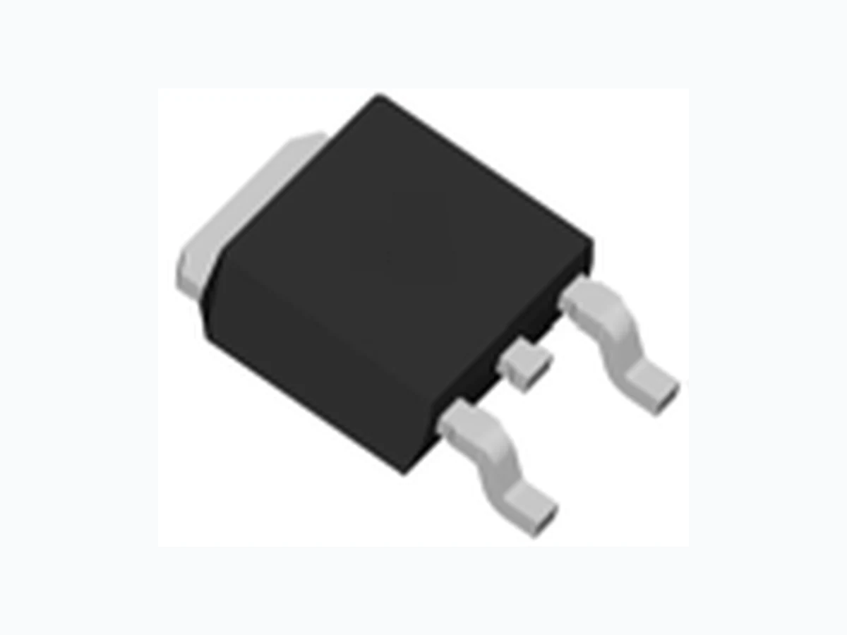
The 15N10G uses advanced trench technology to provide excellent R DS(ON) , low gate charge and operation with gate voltages as low as 4.5V. This device is suitable for use as a Battery protection or in other switching application. General Features ƽ ƽ High power and current handing capability ƽ Lead free product is acquired ƽ Surface mount package Application ƽBattery switch ƽDC/DC converter Absolute Maximum Ratings (T A =25ćunless otherwise noted) Parameter Symbol Limit Unit Drain-Source Voltage V DS 100 V Gate-Source Voltage V GS ±20 V Drain Current-Continuous I D 12 A Drain Current-Pulsed (Note 1) I DM 30 A Maximum Power Dissipation P D 30 W Operating Junction and Storage Temperature Range T J STG -55 To 175 ć Thermal Characteristic R θJC 5 /Wć Drain Current-Continuous 8.4 A T C =100° C T C =25° C Maximum Power Dissipation 15 W T C =25° C G S D T C =100° C Thermal Resistance,Junction-to-Case (Note 2) V D S S R D S O N I D 135 A 10V @ (typ) Ωm100V 12A 120 10V www.sztuofeng.com ,2018 V1.01 Mar N -CHANNEL ENHANCEMENT MODE POWER MOSFET SHENZHENTUOFENGSEMICONDUCTORTECHNOLOGYCO.,LTD 15N10G D G S TO -252 15N10G TFYWCP MARKING EquivalentCircuit Y :year code W :week code
Notes: 1. Repetitive Rating: Pulse width limited by maximum junction temperature. 2. Surface Mounted on FR4 Board, t ≤ 10 sec. 3. Pulse Test: Pulse Width ≤ 300μs, Duty Cycle ≤ 2 . % 4. Guaranteed by design, not subject to production Electrical Characteristics (T C =25℃unless otherwise noted) Parameter Symbol Condition Min Typ Max Unit Off Characteristics Drain-Source Breakdown Voltage BV DSS V GS =0V I D =250μA 100 107 - V Zero Gate Voltage Drain Current I DSS V DS =100V,V GS =0V - - 1 μA Gate-Body Leakage Current I GSS V GS =±20V,V DS =0V - - ±100 nA On Characteristics (Note 3) Gate Threshold Voltage V GS(th) V DS GS D =250μA 1.2 1.8 2.5 V Drain-Source On-State Resistance R DS(ON) V GS =10V, I D =6A Ω Forward Transconductance g FS V DS =25V,I D =6A 3.5 - - S Dynamic Characteristics (Note4) Input Capacitance C lss 206 Output Capacitance C oss Reverse Transfer Capacitance C rss V DS =25V,V GS =0V, F=1.0MHz Switching Characteristics (Note 4) Turn-on Delay Time t d(on) nS Turn-on Rise Time t r Turn-Off Delay Time t d(off) Turn-Off Fall Time t f V DD =50V,I D V GS =10V,R G =2Ω Total Gate Charge Q g nC Gate-Source Charge Q gs Gate-Drain Charge Q gd V DS =50V,I D =5A, V GS =10V Drain-Source Diode Characteristics Diode Forward Voltage (Note 3) V SD V GS =0V,I S =9.6A - - 1.2 V Diode Forward Current (Note 2) I S - - 12 A Reverse Recovery Time t rr - 21 nS Reverse Recovery Charge Qrr TJ = 25°C, IF =5.6A di/dt = 100A/μs (Note3) - 97 nC Forward Turn-On Time t on Intrinsic turn-on time is negligible (turn-on is dominated by LS+LD) Drain-Source On-State Resistance R DS(ON) V GS =4.5V, I D =6A Ω www.sztuofeng.com ,2018 V1.02 Mar N -CHANNEL ENHANCEMENT MODE POWER MOSFET SHENZHENTUOFENGSEMICONDUCTORTECHNOLOGYCO.,LTD 15N10G 0.136 0.146 0.120 0.130 PF PF PF 28.6 1.6 - - 14.7 nS - - 3.5 nS - - 20.9 nS - - 2.7 =5A, - - 4.3 nC - - 1.5 nC - - 1.1
N -CHANNEL ENHANCEMENT MODE POWER MOSFET Fe ,2018 V1.15
Package Information
UNIT: mm 0.25 GAUGE PLANE L VIEW A SEATING PLANE D E e H A SEE VIEW A b c SYMBOL MIN. MAX. 2.39 4.95 5.46 0.46 0.61 0.13 5.33 A c D E MILLIMETERS b 0.50 0.89
2.29 BSC
4.57 6.35 6.73 6.22
0.090 BSC
MIN. MAX. INCHES 0.094 0.020 0.035 0.195 0.215 0.018 0.024 0.210 0.180 0.250 0.265 2.18 0.245 0.086 0.005 0.035 0.070 0.410 H L e 9.40 0.90 0.46 0.89 1.78 10.41 0.370 0.035 0.018 0.040L4 1.02 0.1503.81 0.89 2.03 0.035 0.080 0 8°0° 8°0° 6.00 6.00 0.236 0.236 6.8 MIN. 3 MIN. 6.25 MIN. 6.6 1.5 MIN. 2.286 4.572 www.sztuofeng.com SHENZHENTUOFENGSEMICONDUCTORTECHNOLOGYCO.,LTD 15N10G