

 Download PDF
UDD32CXXL01 YAGEO
Document overview
- PDF pages: 8
Technical content
Page 1
DATA SHEET
ELECTROSTATIC DISCHARGE PROTECTION DEVICES INDUSTRIAL / CONSUMER
RoHS compliant & Halogen free
Page 2
Electrostatic Discharged Protection Devices (ESD) Data Sheet
Description
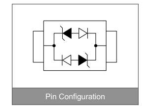
The series are an ultra low capacitance TVS array designed to protect high speed data interfaces. This series has been specifically designed to protect sensitive components which are connected to data an trans- -mission lines from overvoltage caused by electrostatic discharge (ESD), cable discharge events (CDE) and lightning. The unique design incorporates surge rated, low capacitance steering diodes and a TVS diode in a single package. During transient conditions, the steering diodes direct the transient current to ground. The internal TVS diode clamps the transient voltage to a safe level. The ultra low capacitance array configuration allows the user to protect up to the high
speed data lines. These devices are in a signal package, RoHS/WEEE compliant, SOD-323 package. It measures 2.5×1.25×1.0mm. The series devices may be used to meet the immunity requirements of IEC61000-4-2 (ESD), IEC61000-4-4 (EFT) and IEC61000-4-5 (Surge).
Features
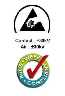
- IEC61000-4-2 ESD 30KV Air, 30KV contact compliance ESD 15KV Air, 8KV contact compliance for UDD32C36L01
- SOD-323 surface mount package
- Protects one I/O line
- Working voltage: 3V, 5V, 8V, 12V ,15V, 24V, 36V
- Low leakage current
- Low operating and clamping voltages
- Solid-state silicon avalanche technology
- Lead Free/RoHS compliant
- Solder reflow temperature: Pure Tin-Sn, 260~270℃
- Flammability rating UL 94V-0
- Meets MSL level 1, per J-STD-020
Applications
- USB 2.0 and USB 3.0 interface
- 10/100/1000 Ethernet
- Personal digital assistants (PDA)
- Serial ATA protection
- Digital visual interface (DVI)
- Wireless system devices
- Handhelds and notebooks
- Digital cameras
- RF interface
Page 3
Maximum Ratings
| Rating | Symbol | Value | Unit |
|---|---|---|---|
| Peak pulse power (tp=8/20μs waveform) | P PP | 350 | W |
| ESD voltage (Contact discharge) | V ESD | ±30 | kV |
| ESD voltage (Air discharge) | ±30 | ||
| Storage & operating temperature range | T ,T STG J | -55~+150 | ℃ |
Electrical Characteristics (TJ=25℃)
UDD32C03L01 (Marking: AC)
| Parameter | Symbol | Condition | Min. | Typ. | Max. | Unit |
|---|---|---|---|---|---|---|
| Reverse stand-off voltage | V RWM | 3.3 | V | |||
| Reverse breakdown voltage | V BR | I =1mA BR | 4 | V | ||
| Reverse leakage current | I R | V =3.3V R | 5 | μA | ||
| Clamping voltage (tp=8/20μs) | V C | I =1A PP | 7 | V | ||
| Clamping voltage (tp=8/20μs) | V C | I =5A PP | 15 | V | ||
| Peak Pulse Current (tp=8/20μs) | I PP | 19 | A | |||
| Off state junction capacitance | C J | 0Vdc,f=1MHz | 0.8 | pF |
UDD32C05L01 (Marking: BC)
| Parameter | Symbol | Condition | Min. | Typ. | Max. | Unit |
|---|---|---|---|---|---|---|
| Reverse stand-off voltage | V RWM | 5 | V | |||
| Reverse breakdown voltage | V BR | I =1mA BR | 6 | V | ||
| Reverse leakage current | I R | V =5V R | 5 | μA | ||
| Clamping voltage (tp=8/20μs) | V C | I =1A PP | 9.8 | V | ||
| Clamping voltage (tp=8/20μs) | V C | I =5A PP | 18.3 | V | ||
| Peak Pulse Current (tp=8/20μs) | I PP | 17 | A | |||
| Off state junction capacitance | C J | 0Vdc,f=1MHz | 0.8 | pF |
UDD32C08L01(Marking: BC.)
| Parameter | Symbol | Condition | Min. | Typ. | Max. | Unit |
|---|---|---|---|---|---|---|
| Reverse stand-off voltage | V RWM | 8 | V | |||
| Reverse breakdown voltage | V BR | I =1mA BR | 8.5 | V | ||
| Reverse leakage current | I R | V =8V R | 1 | μA | ||
| Clamping voltage (tp=8/20μs) | V C | I =1A PP | 13 | V | ||
| Clamping voltage (tp=8/20μs) | V C | I =10A PP | 24 | V | ||
| Peak Pulse Current (tp=8/20μs) | I PP | 17 | A | |||
| Off state junction capacitance | C J | 0Vdc,f=1MHz | 1 | pF |
Page 4
UDD32C12L01 (Marking: DC)
| Parameter | Symbol | Condition | Min. | Typ. | Max. | Unit |
|---|---|---|---|---|---|---|
| Reverse stand-off voltage | V RWM | 12 | V | |||
| Reverse breakdown voltage | V BR | I =1mA BR | 13.3 | V | ||
| Reverse leakage current | I R | V =12V R | 1 | μA | ||
| Clamping voltage (tp=8/20μs) | V C | I =1A PP | 19 | V | ||
| Clamping voltage (tp=8/20μs) | V C | I =5A PP | 28.6 | V | ||
| Peak Pulse Current (tp=8/20μs) | I PP | 7 | A | |||
| Off state junction capacitance | C J | 0Vdc,f=1MHz | 0.8 | pF |
UDD32C15L01 (Marking: EC)
| Parameter | Symbol | Condition | Min. | Typ. | Max. | Unit |
|---|---|---|---|---|---|---|
| Reverse stand-off voltage | V RWM | 15 | V | |||
| Reverse breakdown voltage | V BR | I =1mA BR | 16.7 | V | ||
| Reverse leakage current | I R | V =15V R | 1 | μA | ||
| Clamping voltage (tp=8/20μs) | V C | I =1A PP | 24 | V | ||
| Clamping voltage (tp=8/20μs) | V C | I =5A PP | 35 | V | ||
| Peak Pulse Current (tp=8/20μs) | I PP | 6 | A | |||
| Off state junction capacitance | C J | 0Vdc,f=1MHz | 0.8 | pF |
UDD32C24L01 (Marking: HC)
| Parameter | Symbol | Condition | Min. | Typ. | Max. | Unit |
|---|---|---|---|---|---|---|
| Reverse stand-off voltage | V RWM | 24 | V | |||
| Reverse breakdown voltage | V BR | I =1mA BR | 26.7 | V | ||
| Reverse leakage current | I R | V =24V R | 1 | μA | ||
| Clamping voltage (tp=8/20μs) | V C | I =1A PP | 43 | V | ||
| Clamping voltage (tp=8/20μs) | V C | I =5A PP | 56 | V | ||
| Peak Pulse Current (tp=8/20μs) | I PP | 6 | A | |||
| Off state junction capacitance | C J | 0Vdc,f=1MHz | 0.8 | pF |
Page 5
UDD32C36L01 (Marking: KC)
| Parameter | Symbol | Condition | Min. | Typ. | Max. | Unit |
|---|---|---|---|---|---|---|
| Reverse stand-off voltage | V RWM | 36 | V | |||
| Reverse breakdown voltage | V BR | I =1mA BR | 40 | V | ||
| Reverse leakage current | I R | V =36V R | 1 | μA | ||
| Clamping voltage (tp=8/20μs) | V C | I =1A PP | 70 | V | ||
| Clamping voltage (tp=8/20μs) | V C | I =2A PP | 75 | V | ||
| Peak Pulse Current (tp=8/20μs) | I PP | 3 | A | |||
| Off state junction capacitance | C J | 0Vdc,f=1MHz | 0.8 | pF |
Typical Characteristics Curves
Figure 1. Power Derating Curve
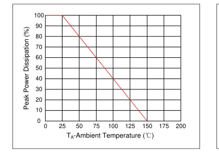
Figure 3. Non-Repetitive Peak Pulse vs Pulse Time
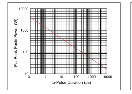
Figure 2. Pulse Waveform
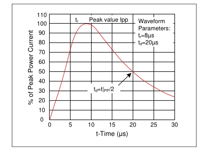
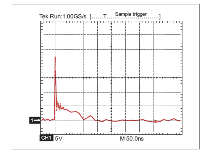
Figure 4. ESD Clamping (8kV Contact IEC61000-4-2)
Page 6
Recommended Soldering Conditions
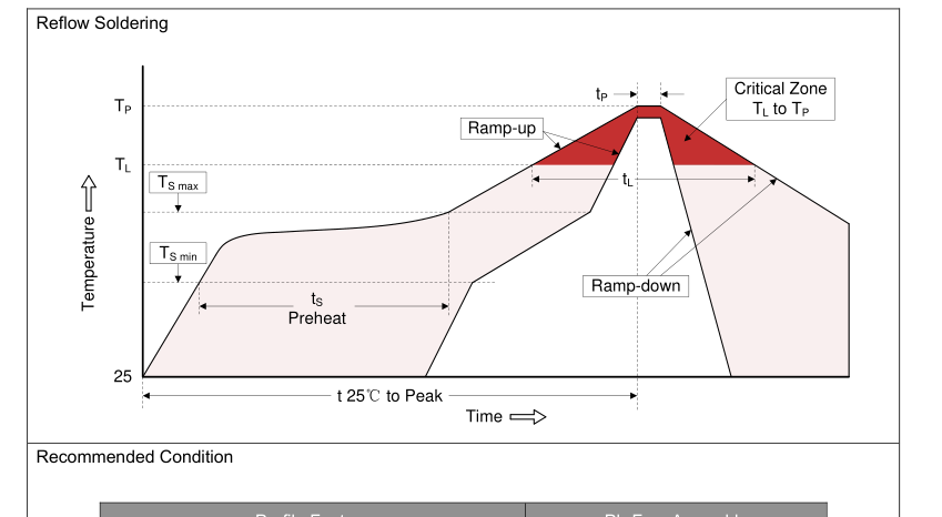
| Profile Feature | Pb-Free Assembly |
| Average ramp-up rate (T to T ) L P | 3℃/second max. |
| Preheat -Temperature Min (T ) S min -Temperature Max (T ) S max -Time (min to max) (ts) | 150℃ 200℃ 60-180 seconds |
| T to T S max L -Ramp-up Rate | 3℃/second max. |
| Time maintained above: -Temperature (T ) L -Time (t ) L | 217℃ 60-150 seconds |
| Peak Temperature (T ) P | 260℃ |
| Time within 5℃ of actual Peak Temperature (t ) P | 20-40 seconds |
| Ramp-down Rate | 6℃/second max. |
| Time 25℃ to Peak Temperature | 8 minutes max. |
Page 7
Dimensions (SOD-323)
| G E H X 1 2 A F D B C detail X 0.50 (2X) 0.60 (2X) 2.3 Recommended Soldering Pad Layout | Symbol | Dimension | |||
| Millimeters | Inches | ||||
| Min. | Max. | Min. | Max. | ||
| A | 0.80 | 1.10 | 0.031 | 0.043 | |
| B | 0.00 | 0.10 | 0.000 | 0.004 | |
| C | 0.20 | - | 0.008 | - | |
| D | 0.11 | 0.20 | 0.004 | 0.008 | |
| E | 1.15 | 1.35 | 0.045 | 0.053 | |
| F | 0.25 | 0.35 | 0.010 | 0.014 | |
| G | 1.60 | 1.80 | 0.063 | 0.071 | |
| H | 2.40 | 2.70 | 0.094 | 0.102 | |
Packaging
| Tape øD0 P0 P1 P2 K E F W B0 B A0 øD1 A t | Symbol | Dimension (mm) |
| W | 8.00±0.30 | |
| P0 | 4.00±0.10 | |
| P1 | 4.00±0.10 | |
| P2 | 2.00±0.10 | |
| D0 | Φ1.55±0.10 | |
| D1 | Φ1.00±0.05 | |
| E | 1.75±0.10 | |
| F | 3.50±0.10 | |
| A | 1.48±0.10 | |
| A0 | 0.80±0.10 | |
| B | 3.00±0.10 | |
| B0 | 1.80±0.10 | |
| K | 1.05±0.10 | |
| t | 0.25±0.05 | |
| Reel D2 D W1 | D | Φ178.0±2.0 |
| D2 | Φ13.0 | |
| W1 | 9.5 | |
| Quantity: 3000PCS | ||
Page 8
Product specification
Circuit Protection Components
LEGAL DISCLAIMER
YAGEO, its distributors and agents (collectively, “YAGEO”), hereby disclaims any and all liabilities for any errors, inaccuracies or incompleteness contained in any product related information, including but not limited to product specifications, datasheets, pictures and/or graphics. YAGEO may make changes, modifications and/or improvements to product related information at any time and without notice.
YAGEO makes no representation, warranty, and/or guarantee about the fitness of its products for any particular purpose or the continuing production of any of its products. To the maximum exten t permitted by law, YAGEO disclaims (i) any and all liability arising out of the application or use of any YAGEO product, (ii) any and all liability, including without limitation special, consequential or incidental damages, and (iii) any and all implied warranties, including warranties of fitness for a particular purpose, non -infringement and merchantability.
YAGEO products are designed for general purpose applications under normal operation and usage conditions. Please contact YAGEO for the applications listed below which require especially high reliability for the prevention of defects which might directly cause damage to the third party's life, body or property: Aerospace equipment (artificial satellite, rocket, etc.), Atomic energy-related equipment, Aviation equipment, Disaster prevention equipment, crime prevention equipment, Electric heating apparatus, burning equipment, Highly public information network equipment, data-processing equipment , Medical devices, Military equipment, Power generation control equipment, Safety equipment, Traffic signal equipment, Transportation equipment and
Undersea equipment, or for any other application or use in which the failure of YAGEO products could result in personal injury or death, or serious property damage. Particularly YAGEO Corporation and its affiliates do not recommend the use of commercial or automotive grade products for high reliability applications or manned space flight.
Information provided here is intended to indicate product specifications only. YAGEO reserves all the rights for revising this content without further notification, as long as products are unchanged. Any product change will be announced by PCN.