

U6084B ATMEL
Document overview
- PDF pages: 10
Technical content
Page 1

Features
- Pulse-width Modulation up to 2 kHz Clock Frequency
- Protection against Short-circuit, Load-dump Overvoltage and Reverse VS
- Duty-cycle 0 to 100% Continuously
- Output Stage for Power MOSFET
- Interference and Damage Protection According to VDE 0839 and ISO/TR 7637/1
- Charge-pump Noise Suppressed
- Ground-wire Breakage Protection
Description
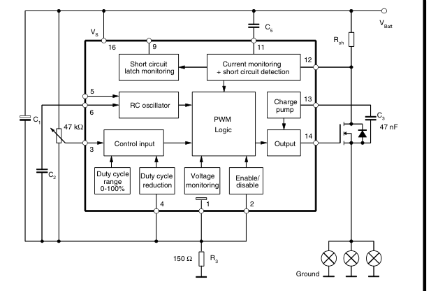
The U6084B is a PWM-IC with bipolar technology designed for the control of an N-channel power MOSFET used as a high-side switch. The IC is ideal for use in the brightness control (dimming) of lamps such as in dashboard applications. For constant brightness, the preselected duty-cycle can be reduced automatically as a function of the supply voltage.
Figure 1. Block Diagram with External Circuit
Page 2
Pin Configuration
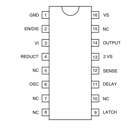
Figure 2. Pinning
Pin Description
| Pin | Symbol | Function |
|---|---|---|
| 1 | GND | IC ground |
| 2 | EN/DIS | Enable/disable |
| 3 | VI | Control input (duty cycle) |
| 4 | REDUCT | Duty cycle reduction |
| 5 | NC | Attenuation |
| 6 | OSC | Oscillator |
| 7 | NC | Not connected |
| 8 | NC | Not connected |
| 9 | LATCH | Status short-circuit latch |
| 10 | NC | Not connected |
| 11 | DELAY | Short-circuit protection delay |
| 12 | SENSE | Current sensing |
| 13 | 2VS | Voltage doubler |
| 14 | OUTPUT | Output |
| 15 | NC | Not connected |
| 16 | VS | Supply voltage V S |
Page 3
Functional Description
Pin1 – GND
To protect the FET in case of ground-wire breakage, a 820 kΩ resistor between gate
Ground-wire Breakage
and source is recommended to provide proper switch-off conditions.
Pin 2 – Enable/Disable
The dimmer can be switched on or off, with pin 2, independently of the set duty cycle.
Table 1. Pin 2 Function
| V 2 | Function |
| Approximately > 0.7 V or open | Disable |
| < 0.7 V or connected to pin 1 | Enable |
The pulse width is controlled by means of an external potentiometer (47 kΩ). The char-
Pin 3 – Control Input
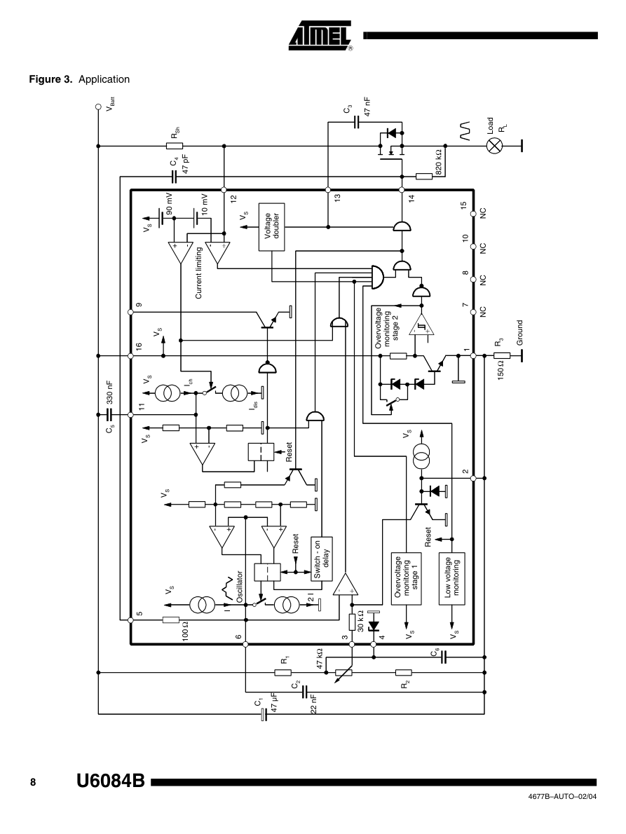
acteristic (angle of rotation/duty cycle) is linear. The duty cycle be varied from 0 to 100%. It is possible to further restrict the duty cycle with resistors R1 and R2 (see Figure 3 on page 8).
Pin 3 is protected against short-circuit to VBatt and ground GND (VBatt ≤16.5 V).
Pin 4 – Duty Cycle
With pin 4 connected according to Figure 3 on page 8, the set duty cycle is reduced to VBatt ≈ 12.5 V. This causes a power reduction in the FET and in the lamps. In addition,
Reduction
the brightness of the lamps is largely independent of the supply voltage range, VBatt = 12.5 to 16 V.
The rise and fall time (tr, tf) of the lamp voltage can be limited to reduce radio interfer-
Output Slope Control
ence. This is done with an integrator which controls a power MOSFET as source follower. The slope time is controlled by an external capacitor C4 and the oscillator current (see Figure 3 on page 8).
Calculation:
C4 × ---------
= = tf tr VBatt
Iosc
With VBatt = 12 V, C4 = 470 pF and Iosc = 40 µA, we thus obtain a controlled slope of
470 pF
= = 12 V ×
× 141 µs ------------------
tf tr
40 µA
Pin 5 – Attenuation
Capacitor C4 connected to pin 5 damps oscillation tendencies.
Pin 6 – Oscillator
The oscillator determines the frequency of the output voltage. This is defined by an external capacitor, C2. It is charged with a constant current, I, until the upper switching threshold is reached. A second current source is then activated which taps a double current, 2 × I, from the charging current. The capacitor, C2, is thus discharged by the current, I, until the lower switching threshold is reached. The second source is then switched off again and the procedure starts once more.
Page 4
Example for Oscillator
VT100 VS α1 VBatt IS = × = (
– × R3 α1 ) ×
Frequency Calculation
VT<100 VS α2 VBatt IS = × = (
– × R3 α2 ) ×
VTL VS α3 VBatt IS R3 = × = (
– × ) × α3
where
VT100 = High switching threshold 100% duty cycle VT<100 = High switching threshold < 100% duty cycle VTL = Low switching threshold α1, α2 and α3 are fixed values The above mentioned threshold voltages are calculated for the following values given in the datasheet. VBatt = 12 V, IS = 4 mA, R3 = 150 Ω, α1 = 0.7, α2 = 0.67 and α3 = 0.28. VT100 = (12 V - 4 mA × 150 Ω) × 0.7 ≈ 8 V VT<100 = 11.4 V × 0.67 = 7.6 V VTL = 11.4 V × 0.28 = 3.2 V For a duty cycle of 100%, the oscillator frequency, f, is as follows:
Iosc
f = ------------------------------------------------------------ where C2 = 22 nF and Iosc = 40 µA × (
) ×
2 VT100 VTL C2 –
Therefore:
40 µA
f = ------------------------------------------------------------------- =
189 Hz
× (
) ×
2 8 V – 3.2 V 22 nF
For a duty cycle of less than 100%, the oscillator frequency, f, is as follows:
Iosc
f = ----------------------------------------------------------------------------------------------------------- × (
) × × ×
2 VT<100 VTL C2
+ 4 VBatt C4
–
where C4 = 470 pF
40 µA
f = -------------------------------------------------------------------------------------------------------------------------------
= 185 Hz
× (
) ×
× ×
2 7.6 V – 3.2 V 22 nF
+ 4 12 V 470 pF
A selection of different values of C2 and C4 provides a range of oscillator frequencies from 10 to 2000 Hz.
Pins 7, 8, 10 and 15
Not connected.
Pin 9 – Status Short
The status of the short-circuit latch can be monitored via pin 9 (open collector output).
Circuit Latch
Table 2. Pin 9 Function
| Pin 9 | Function |
| L | Short-circuit detected |
| H | Not short-circuit detected |
Page 5
Pins 11 and 12 – Short-circuit Protection and Current Sensing
The lamp current is monitored by means of an external shunt resistor. If the lamp current
Short-circuit Detection and
exceeds the threshold for the short-circuit detection circuit (VT2 ≈ 90 mV), the duty cycle
Time Delay td
is switched over to 100% and capacitor C5 is charged by a current source of 20 µA (Ich - Idis). The external FET is switched off after the cut-off threshold (VT11) is reached. Renewed switching on the FET is possible only after a power-on reset. The current source, Idis, ensures that capacitor C5 is not charged by parasitic currents. Capacitor C5 is discharged by Idis to typ. 0.7 V. Time delay, td, is as follows:
( ) V11 – 0.7 V
= × ---------------------------------- td C5 ( ) Ich Idis –
With C5 = 330 nF and VBatt = 12 V, we have
(
)
9.8 V – 0.7 V
= 330 nF × --------------------------------------
td
= 150 ms 20 µA
The lamp current is limited by a control amplifier that protects the external power transis-
Current Limitation
tor. The voltage drop across an external shunt resistor acts as the measured variable. Current limitation takes place for a voltage drop of VT1 ≈ 100 mV. Owing to the difference VT - VT2 ≈ 10 mV, current limitation occurs only when the short-circuit detection circuit has responded.
After a power-on reset, the output is inactive for half an oscillator cycle. During this time, the supply voltage capacitor can be charged so that current limitation is guaranteed in the event of a short-circuit when the IC is switched on for the first time.
Pins 13 and 14 – Charge
Pin 14 (output) is suitable for controlling a power MOSFET. During the active integration phase, the supply current of the operational amplifier is mainly supplied by capacitor C3
Pump and Output
(bootstrapping). Additionally, a trickle charge is generated by an integrated oscillator (f13 ≈ 400 kHz) and a voltage doubler circuit. This permits a gate voltage supply at a duty cycle of 100%.
Pin 16 – Supply Voltage,
Vs or VBatt
In the event of voltages of approximately VBatt < 5.0 V, the external FET is switched off
Undervoltage Detection
and the latch for short-circuit detection is reset. A hysteresis ensures that the FET is switched on again at approximately VBatt ≥ 5.4 V.
Overvoltage Detection
If overvoltages of VBatt > 20 V (typically) occur, the external transistor is switched off and
Stage 1
switched on again at VBatt < 18.5 V (hysteresis).
If VBatt > 28.5 V (typically), the voltage limitation of the IC is reduced from 26 V to 20 V.
Stage 2
The gate of the external transistor remains at the potential of the IC ground, thus producing voltage sharing between the FET and lamps in the event of overvoltage pulses (e.g., load-dump). The short-circuit protection is not in operation. At VBatt < 23 V, the overvoltage detection stage 2 is switched off.
Page 6
Absolute Maximum Ratings
Stresses beyond those listed under “Absolute Maximum Ratings” may cause permanent damage to the device. This is a stress rating only and functional operation of the device at these or any other conditions beyond those indicated in the operational sections of this specification is not implied. Exposure to absolute maximum rating conditions for extended periods may affect device reliability
| Parameters | Symbol | Value | Unit |
|---|---|---|---|
| Junction temperature | T j | 150 | °C |
| Ambient temperature range | T amb | -40 to +110 | °C |
| Storage temperature range | T stg | -55 to +125 | °C |
Thermal Resistance
| Parameters | Symbol | Value | Unit |
|---|---|---|---|
| Junction ambient | R thJA | 120 | K/W |
Electrical Characteristics
Tamb = -40 to +110°C, VBatt = 9 to 16.5 V, (basic function is guaranteed between 6.0 V to 9.0 V) reference point ground, unless otherwise specified (see Figure 1 on page 1). All other values refer to pin GND (pin 1).
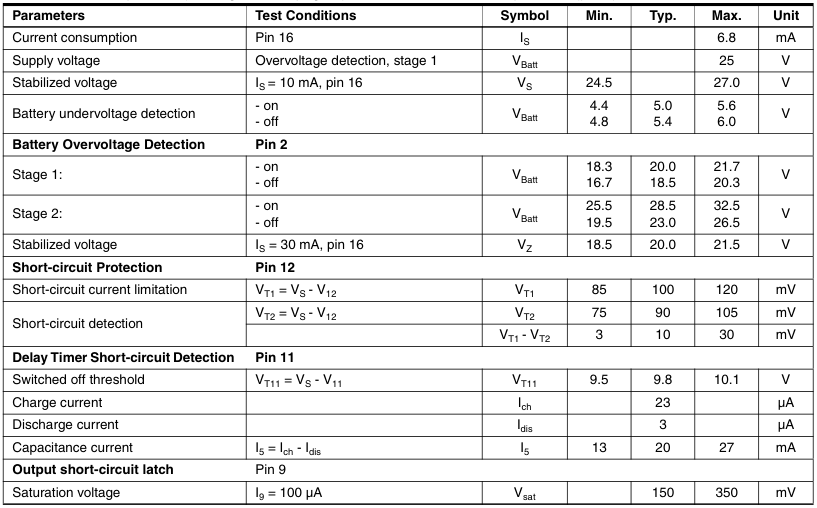
Notes: 1. Reference point is battery ground
Page 7
Electrical Characteristics (Continued)
Tamb = -40 to +110°C, VBatt = 9 to 16.5 V, (basic function is guaranteed between 6.0 V to 9.0 V) reference point ground, unless otherwise specified (see Figure 1 on page 1). All other values refer to pin GND (pin 1).
| Parameters | Test Conditions | Symbol | Min. | Typ. | Max. | Unit |
|---|---|---|---|---|---|---|
| Voltage Doubler Pin 13 | ||||||
| Voltage | Duty cycle 100% | V 13 | 2 V S | |||
| Oscillator frequency | f 13 | 280 | 400 | 520 | kHz | |
| Internal voltage limitation | I = 5 mA 13 | V 13 | 26 | 27.5 | 30.0 | V |
| (whichever is lower) | V 13 | (V ) S+14 | (V ) S+15 | (V ) S+16 | ||
| Gate Output Pin 14 | ||||||
| Voltage | Low level | V 14 | 0.35 | 0.70 | 0.95 | V |
| V = 16.5 V, T = 110°C, Batt amb R = 150 Ω 3 | 1.5(1) | |||||
| High level, duty cycle 100% | V 14 | V 13 | ||||
| Current | V = Low level 14 | I 14 | 1.0 | mA | ||
| V = High level, I > I 14 14 13 | -1.0 | |||||
| Enable/Disable Pin 2 | ||||||
| Current | V = 0 V 2 | I 2 | -20 | -40 | -60 | µA |
| Duty Cycle Reduction Pin 4 | ||||||
| Z-voltage | I = 500 µA 4 | V 4 | 6.9 | 7.4 | 8.0 | V |
| Oscillator | ||||||
| Frequency | Pin6 | f | 10 | 2000 | Hz | |
| Threshold cycle Upper Lower | V V = High, α = -----T---1--0---0- 14 1 V S | α 1 | 0.68 | 0.7 | 0.72 | |
| V V = Low, α = -----T---<--1---0---0- 14 2 V S | α 2 | 0.65 | 0.67 | 0.69 | ||
| V α = -----T---L- 3 V S | α 3 | 0.26 | 0.28 | 0.3 | ||
| Oscillator current | V = 12 V Batt | ±I osc | 26 | 40 | 54 | µA |
| Frequency tolerance | C open, C = 470 nF, 4 2 duty cycle = 50% | f | 6.0 | 9.9 | 13.5 | Hz |
Notes: 1. Reference point is battery ground
Page 8
Page 9
Ordering Information
| Extended Type Number | Package | Remarks |
|---|---|---|
| U6084B-FP | SO16 | – |
Package Information
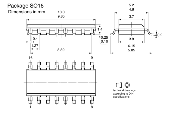
Revision History
Please note that the referring page numbers in this section are referred to the specific revision mentioned, not to this document.
Changes from Rev.
- Block Diagram on page 1 changed.
4677A - 02/03 to Rev.
- New heading rows at Table “Absolute Maximum Ratings” on page 6 added.
4677B - 02/04
Page 10

Atmel Corporation
Atmel Operations
Memory
2325 Orchard Parkway San Jose, CA 95131, USA
2325 Orchard Parkway
Tel: 1(408) 441-0311
San Jose, CA 95131, USA
Fax: 1(408) 487-2600
Tel: 1(408) 441-0311 Fax: 1(408) 436-4314
Regional Headquarters
Microcontrollers 2325 Orchard Parkway
Europe
San Jose, CA 95131, USA
Atmel Sarl
Tel: 1(408) 441-0311
Route des Arsenaux 41
Fax: 1(408) 436-4314
Case Postale 80 CH-1705 Fribourg
La Chantrerie
Switzerland
BP 70602
Tel: (41) 26-426-5555
44306 Nantes Cedex 3, France
Fax: (41) 26-426-5500
Tel: (33) 2-40-18-18-18 Fax: (33) 2-40-18-19-60
Asia Room 1219
ASIC/ASSP/Smart Cards
Chinachem Golden Plaza
Zone Industrielle
77 Mody Road Tsimshatsui
13106 Rousset Cedex, France
East Kowloon
Tel: (33) 4-42-53-60-00
Hong Kong
Fax: (33) 4-42-53-60-01
Tel: (852) 2721-9778 Fax: (852) 2722-1369
1150 East Cheyenne Mtn. Blvd. Colorado Springs, CO 80906, USA
Japan
Tel: 1(719) 576-3300
9F, Tonetsu Shinkawa Bldg.
Fax: 1(719) 540-1759
1-24-8 Shinkawa Chuo-ku, Tokyo 104-0033
Scottish Enterprise Technology Park
Japan
Maxwell Building
Tel: (81) 3-3523-3551
East Kilbride G75 0QR, Scotland
Fax: (81) 3-3523-7581
Tel: (44) 1355-803-000 Fax: (44) 1355-242-743
RF/Automotive Theresienstrasse 2 Postfach 3535 74025 Heilbronn, Germany Tel: (49) 71-31-67-0 Fax: (49) 71-31-67-2340
1150 East Cheyenne Mtn. Blvd. Colorado Springs, CO 80906, USA Tel: 1(719) 576-3300 Fax: 1(719) 540-1759
Biometrics/Imaging/Hi-Rel MPU/ High Speed Converters/RF Datacom Avenue de Rochepleine BP 123 38521 Saint-Egreve Cedex, France Tel: (33) 4-76-58-30-00 Fax: (33) 4-76-58-34-80
Literature Requests www.atmel.com/literature
Disclaimer: Atmel Corporation makes no warranty for the use of its products, other than those expressly contained in the Company’s standard warranty which is detailed in Atmel’s Terms and Conditions located on the Company’s web site. The Company assumes no responsibility for any errors which may appear in this document, reserves the right to change devices or specifications detailed herein at any time without notice, and does not make any commitment to update the information contained herein. No licenses to patents or other intellectual property of Atmel are granted by the Company in connection with the sale of Atmel products, expressly or by implication. Atmel’s products are not authorized for use
as critical components in life support devices or systems.
© Atmel Corporation 2004. All rights reserved. Atmel® and combinations thereof are the registered trademarks of Atmel Corporation or its subsidiaries.
Other terms and product names may be the trademarks of others.
Printed on recycled paper.