
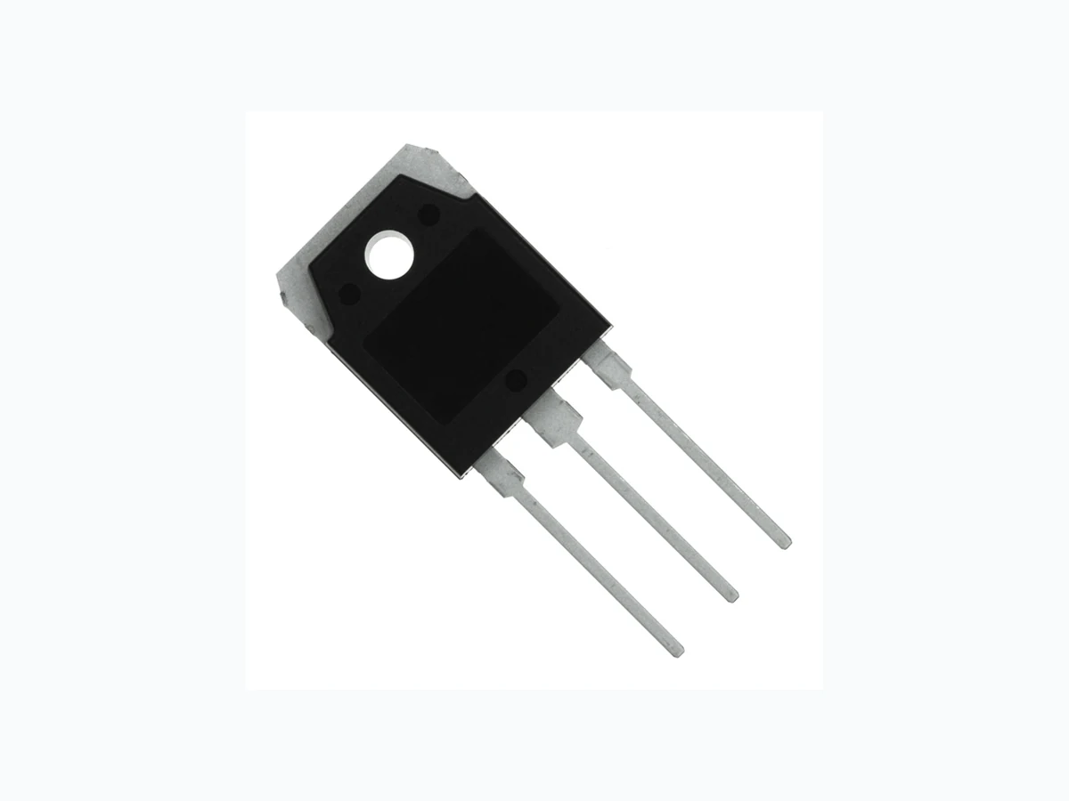
TS20N60PB THINKISEMI
Document overview
- Manufacturer or author: Provided By www.digicamel.com(FREE DATASHEET DOWNLOAD SITE)
- PDF pages: 3
Technical content
Features
R DS(ON) = 0.36 ohm I D = 20A BV DSS = 600V 2. Drain 3. Source 1. Gate General Description This N-channel enhancement mode field-effect power transistor using THINKI Semiconductor advanced planar stripe, DMOS technol- ogy intended for off-line switch mode power supply. Also, especially designed to minimize rds(on) and high rugged avalanche characteristics. The TO-3PB pkg is well suited for adaptor power units,amplifiers,inverters and SMPS application. TO-3PB 20A, 600V, R DS(on) = 0.36 Ω @V GS = 10 V Low gate charge ( typical 14 nC) Low Crss ( typical 20 pF) Fast switching 100% avalanche tested Improved dv/dt capability 175 °C maximum junction temperature rating Electrical Characteristics @ Ta=25℃(unless otherwise specified) a A b s o l u t e M a x i m u m R a t i n g s Symbol Parameter Value Units VDSS Drain-to-Source Breakdown Voltage 600 V ID Drain Current (continuous) at Tc=25℃ 20 A IDM Drain Current (pulsed) 80 A VGS Gate to Source Voltage +/-30 V Ptot Power Dissipation at Tc=25℃ 250 W Derating Factor above 25℃ 2.0 W/℃ Tj Max. Operating Junction Temperature 175 ℃ EAS Single Pulse Avalanche Energy 1200 mJ
b E l e c t r i c a l P a r a m e t e r s Symbol Parameter Test Conditions Min Typ Max Unit VDS Drain-source Voltage VGS =0V, ID=250µA 600 V RDS(on) Static Drain-to-Source on-Resistance VGS =10V, ID=10A 0.36 0.45 Ω VGS(th) Gated Threshold Voltage VDS=VGS, ID=250µA 2.0 4.0 V IDSS Drain to Source leakeage Current VDS=600V, VGS = 0V 1.0 µA IGSS(F) Gated to Source Forward Leakage VGS = +30V 100 nA IGSS(R) Gated to Source Reverse Leakage VGS = -30V -100 nA Ciss Input Capacitance VGS =0V, VDS=25V, f=1.0MHZ 2847 pF Coss Output Capacitance 252 pF Crss Reverse Transfer Capacitance 20 pF c S w i t c h i n g C h a r a c t e r i s t i c s Symbol Parameter Test Conditions Min Typ Max Unit td(on) Turn-on Delay Time VDD=300V,ID=20A, RG=25Ω 36 nS tr Turn-on Rise Time 73 nS td(off) Turn-off Delay Time 166 nS tf Turn-off Fall Time 73 nS Qg Total Gate Charge VDS=300V ID=20A VGS=10V 61 nC Qgs Gate-Source Charge 14 nC Qgd Gate-Drain Charge 24 nC d S o u r c e D r a i n D i o d e C h a r a c t e r i s t i c s Symbol Parameter Test Conditions Min Typ Max Unit ISD S-D Current(Body Diode) 20 A ISDM Pulsed S-D Current(Body Diode) 80 A VSD Diode Forward Voltage VGS =0V, IDS=20A 1.5 V trr Reverse Recovery Time TJ=25℃,IS=20A di/dt=100A/us 425 nS Qrr Reverse Recovery Charge 3.7 µC *Pulse Test: Pulse Width <= 300µs, Duty Cycle< =2% Symbol Parameter Typ Units RθJC Junction-to-Case 0.5 ℃/W RθJA Junction-to-Ambient 40 ℃/W © 2006 Thinki Semiconductor Co., Ltd. http://www.thinkisemi.com/ Page 2/3Rev.08C
Package Information
© 2006 Thinki Semiconductor Co., Ltd. http://www.thinkisemi.com/ Page 3/3Rev.08C