
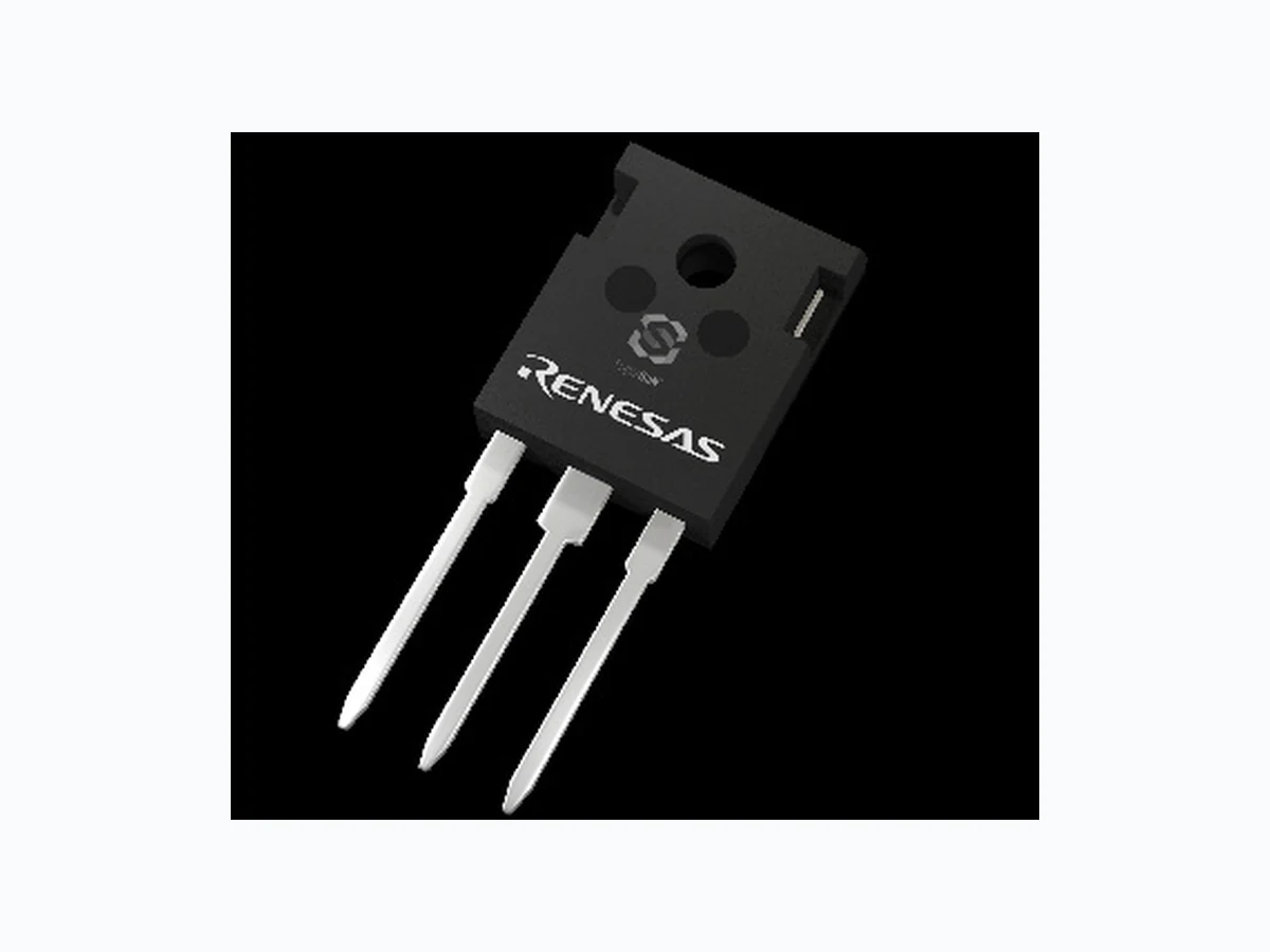
TP65H050G4WS_V01 RENESAS
Document overview
- Manufacturer or author: Provided By www.digicamel.com(free datasheet download site)
- PDF pages: 13
Technical content
Datasheet sections
- 1.1 Pin Assignments
- 1.2 Pin Descriptions
- 2.1 Absolute Maximum Ratings
- 2.2 Thermal Specifications
- 2.3 Electrical Specifications – Forward Device
- 2.4 Electrical Specifications – Reverse Device
Features
■ Ultra-fast switching Gen IV GaN technology ■ JEDEC-qualified GaN technology ■ Dynamic RDS(on)eff production tested ■ Reduced crossover loss ■ Negligible Qrr ■ RoHS compliant and Halogen-free packaging
Applications
■ AI datacenter and telecom power supplies ■ E-mobility charging ■ PV inverter ■ UPS ■ BESS Specifications VDS (V) 650 VDSS(TR)(V) maximum 800 RDS(on) (mΩ) maximum [1] 60 QOSS (nC) typical 120 QG (nC) typical 15.3 1. Dynamic RDS(on) (see Figure 17 and Figure 18)
1.1 Pin Assignments
Figure 1. Pin Assignments
1.2 Pin Descriptions
R07DS1676EU0200 Rev.2.00 Nov 26, 2025 Page 4 2. Specifications
2.1 Absolute Maximum Ratings
Tc = 25°C unless otherwise stated. Caution: Do not operate at or near the maximum ratings listed for extended periods of time. Exposure to such conditions can adversely impact product reliability and result in failures not covered by warranty. Symbol Parameter Limit Value Unit VDSS Drain to source voltage (TJ = -55°C to 150°C) 650 V VDSS(TR) Transient drain to source voltage [1] 800 VGSS Gate to source voltage +20 PD Maximum power dissipation at TC = 25°C 119 W ID Continuous drain current at TC = 25°C 34 A Continuous drain current at TC = 100°C 22 A IDM Pulsed drain current (pulse width: 10µs) 150 A TJ Junction operating temperature -55 to +150 °C TS Storage temperature -55 to +150 °C TSOLD Reflow soldering temperature [2] 260 °C - Mounting torque 80 N cm 1. In off-state, spike duty cycle D < 0.01, spike duration < 30µs, non-repetitive. 2. For 10 sec., 1.6mm from the case.
2.2 Thermal Specifications
Symbol Condition Typical Value Unit RΘJC Junction-to-case 1.05 °C/W RΘJA Junction-to-ambient 40
R07DS1676EU0200 Rev.2.00 Nov 26, 2025 Page 5
2.3 Electrical Specifications – Forward Device
TJ = 25°C unless otherwise stated. Symbol Parameter Test Conditions Minimum Typical Maximum Unit VDSS(BL) Maximum drain-source voltage VGS = 0V 650 - - V VGS(th) Gate threshold voltage VDS = VGS, ID = 0.7mA 3.3 4 4.8 V ΔVGS(th)/TJ Gate threshold voltage temperature coefficient - -6.2 - mV/°C RDS(on)eff Drain-source on-resistance [1] VGS = 10V, ID = 22A, TJ = 25°C - 50 60 mΩ VGS = 10V, ID = 22A, TJ = 150°C - 105 - IDSS Drain-to-source leakage current VDS = 650V, VGS = 0V, TJ = 25°C - 4 40 µA VDS = 650V, VGS = 0V, TJ = 150°C - 15 - IGSS Gate-to-source forward leakage current VGS = 20V - - 100 nA Gate-to-source reverse leakage current VGS = -20V - - -100 CISS Input capacitance VGS = 0V, VDS = 400V, f = 1MHz - 1000 - pF COSS Output capacitance - 110 - CRSS Reverse transfer capacitance - 6 - CO(er) Output capacitance, energy related [2] VGS = 0V, VDS = 0V to 400V - 164 - pF CO(tr) Output capacitance, time related [3] - 280 - QG Total gate charge VDS = 400V, VGS = 0V to 10V, ID = 22A - 15.3 - nC QGS Gate-source charge - 6 - QGD Gate-drain charge - 5 - QOSS Output charge VGS = 0V, VDS = 0V to 400V - 120 - nC tD(on) Turn-on delay VDS = 400V, VGS = 0V to 10V, ID = 22A, RG = 45Ω, ZFB = 240Ω at 100MHz (see Figure 15) - 49.2 - ns tR Rise time - 11.3 - tD(off) Turn-off delay - 88.3 - tF Fall time - 10.9 - 1. Dynamic RDS(on), 100% tested; see Figure 17 and Figure 18 for conditions. 2. Equivalent capacitance to give same stored energy from 0V to 400V. 3. Equivalent capacitance to give same charging time from 0V to 400V.
R07DS1676EU0200 Rev.2.00 Nov 26, 2025 Page 6
2.4 Electrical Specifications – Reverse Device
TJ = 25°C unless otherwise stated. Symbol Parameter Test Conditions Minimum Typical Maximum Unit IS Reverse current VGS = 0V, TC = 100°C, ≤ 25% duty cycle - - 22 A VSD Reverse voltage [1] VGS = 0V, IS = 22A - 2.2 - V VGS = 0V, IS = 11A - 1.6 - 1. Includes dynamic RDS(on) effect. Note: Reverse recovery charge is negligible, enabled by the LV Si FET technology.
Figure 19. TO-247-3 Package Outline Drawing
R07DS1676EU0200 Rev.2.00 Nov 26, 2025 Page 12 6. Related Information All technical documents for Renesas GaN Power devices are accessible from the GaN Power Solutions page. 7. Ordering Information Part Number Package Description Package Configuration TP65H050G4WS TO-247-3 Source tab 8. Revision History Revision Date Description 2.00 Nov 26, 2025 Updated the document's formatting; no technical changes were completed. 1.00 Mar 6, 2022 Initial release.
TOYOSU FORESIA, 3-2-24 Toyosu, Koto-ku, Tokyo 135-0061, Japan www.renesas.com Contact Information For further information on a product, technology, the most up-to-date version of a document, or your nearest sales office, please visit www.renesas.com /contact-us/ . Trademarks Renesas and the Renesas logo are trademarks of Renesas Electronics Corporation. All trademarks and registered trademarks are the property of their respective owners. IMPORTANT NOTICE AND DISCLAIMER RENESAS ELECTRONICS CORPORATION AND ITS SUBSIDIARIES (“RENESAS”) PROVIDES TECHNICAL SPECIFICATIONS AND RELIABILITY DATA (INCLUDING DATASHEETS), DESIGN RESOURCES (INCLUDING REFERENCE DESIGNS), APPLICATION OR OTHER DESIGN ADVICE, WEB TOOLS, SAFETY INFORMATION, AND OTHER RESOURCES “AS IS” AND WITH ALL FAULTS, AND DISCLAIMS ALL WARRANTIES, EXPRESS OR IMPLIED, INCLUDING, WITHOUT LIMITATION, ANY IMPLIED WARRANTIES OF MERCHANTABILITY, FITNESS FOR A PARTICULAR PURPOSE, OR NON-INFRINGEMENT OF THIRD-PARTY INTELLECTUAL PROPERTY RIGHTS. These resources are intended for developers who are designing with Renesas products. You are solely responsible for (1) selecting the appropriate products for your application, (2) designing, validating, and testing your application, and (3) ensuring your application meets applicable standards, and any other safety, security, or other requirements. These resources are subject to change without notice. Renesas grants you permission to use these resources only to develop an application that uses Renesas products. Other reproduction or use of these resources is strictly prohibited. No license is granted to any other Renesas intellectual property or to any third-party intellectual property. Renesas disclaims responsibility for, and you will fully indemnify Renesas and its representatives against, any claims, damages, costs, losses, or liabilities arising from your use of these resources. Renesas' products are provided only subject to Renesas' Terms and Conditions of Sale or other applicable terms agreed to in writing. No use of any Renesas resources expands or otherwise alters any applicable warranties or warranty disclaimers for these products. (Disclaimer Rev.1.01) © 2025 Renesas Electronics Corporation. All rights reserved.