
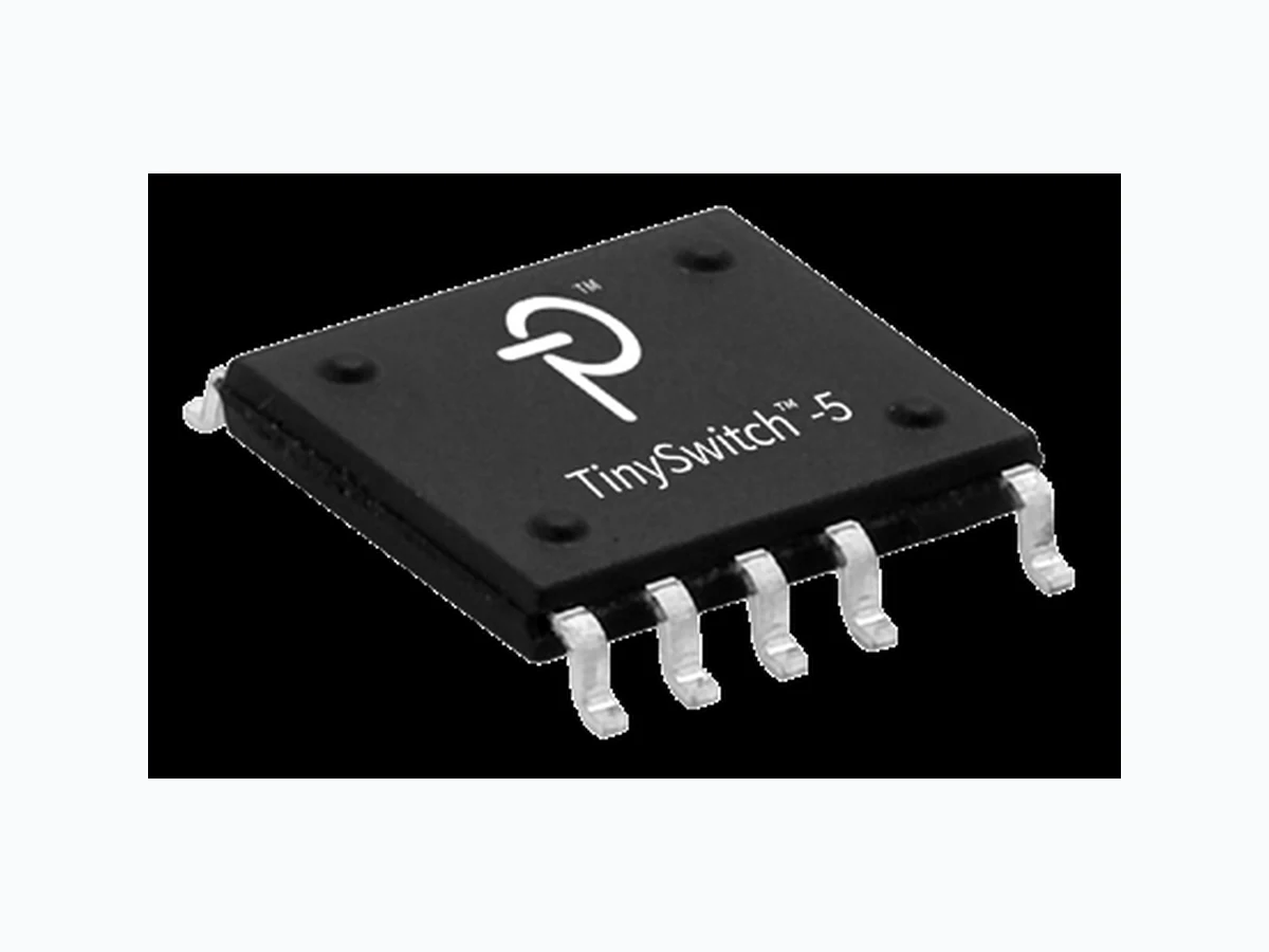
TNY5071K POWERINT
Document overview
- Manufacturer or author: Provided By www.digicamel.com(free datasheet download site)
- PDF pages: 27
Technical content
This Product is Covered by Patents and/or Pending Patent Applications.
- Robust 725 V silicon MOSFET provides excellent surge withstand
- Switching frequency up to 150 kHz minimizes transformer size EcoSmartTM – Energy Efficient
- Up to 92% efficient, flat across load range
- Less than 30 mW no-load power at 230 VAC including line sense
- Up to 210 mW output power for 300 mW input (230 VAC)
- Lossless primary current sensing Reduced Part Count, Design Flexibility
- Frequency jitter reduces EMI filter size
- Integrated soft-start minimizes start-up stress
- Adjustable switching frequency
- ILIM selection without extra components Extensive Protection
- Auto-restart limits power delivery to <3% during overload faults
- Output short-circuit, overload and overvoltage protection
- Line undervoltage (UV) detection prevents turn-off glitching
- Simple, fast AC reset
- Line overvoltage (OV) shutdown
- Accurate thermal shutdown with large hysteresis (OTP) Typical Applications
- Auxiliary, standby and bias power supplies for appliances, and consumer products
- Utility meter, smart grid and industrial power supplies
Figure 1. Typical Flyback Application. Table 1. Power Range by Package Type. Figure 2. Packages.
- Low profile surface mount package ultra-slim designs
- Supports wave or reflow soldering
- PCB cooling via SOURCE pin and exposed pad for low EMI eDIP™-12 Package (V Suffix)
- Low profile horizontal orientation for ultra-slim designs
- Heat transfer to both PCB and heatsink
- Thermal impedance equivalent to a TO-220 package eSIP™-7 Package (E Suffix)
- Vertical orientation for minimum PCB footprint
- Simple heatsink mounting using clip
- Thermal impedance equivalent to TO-220 package
- Provides extended power range Product Type Output Power (W)
400 VDC 230 VAC 85-265 VAC
are subject to change without notice.
400 VDC 230 VAC ±15% 85-265 VAC 400 VDC 230 VAC ±15% 85-265 VAC
Table 2. Output Power Table.
- The power table 2 represents the maximum practical continuous output power based on the following assumptions:
c. 130 V reflected voltage (VOR) and 85% efficiency. d. A 100 VDC minimum DC bus voltage for 85-265 VAC and 300 VDC bus voltage for 230 VAC. e. Sufficient heatsinking to keep device temperature ≤110 °C. f. Power levels shown for the V package device assume 19.4 cm 2 of 610 g/m 2 copper heatsink area. g. Open frame design operating in a +50 °C ambient temperature.
- Minimum peak power capability.
- Packages: E: eSIP-7C, V: eDIP-12B, K: eSOP-12B.
are subject to change without notice. Figure 3. Functional Block Diagram.
are subject to change without notice. Power switch drain connection. undervoltage and overvoltage conditions at the power supply input. This pin should be tied to SOURCE pin to disable UV/OV protection. Feedback control current input pin. Figure 4. Pin Configuration (Top View).
are subject to change without notice. conduction mode (CCM) or discontinuous conduction mode (DCM). blanking, and a silicon MOSFET power switch. energy stored in the BYPASS pin capacitor. than 30 mW in a 5 V output design. threshold, it must rise to VBP to re-enable turn-on of the power switch. The thermal shutdown circuitry senses the power switch temperature. The threshold is set to T SD with a hysteretic response. PCB due to a continuous fault condition. algorithm produces longer off-time as the output load reduces. on-cycle request to turn-on the integrated power switch. and the next switching request. switching frequency (load) increases as shown in Figure 5. continue to increase as load reduces. Figure 5. Normalized Current Limit vs Frequency. at a modulation frequency of f M. approximately 3 cycles at maximum 150 kHz switching frequency. overvoltage sensing and protection. disabled by shorting the VOLTAGE MONITOR pin to the SOURCE pin. brown-in (IUV+) and below the overvoltage shutdown thresholds (I OV+).
Rev. D 03/25 TinySwitch-5 www.power.com This document contains information on a new product. Specifications and information herein are subject to change without notice. PRELIMINARY In normal operation, if the VOLTAGE MONITOR pin current falls below the brown-out threshold (IUV-) and remains below brown-out for longer than tUV-, switching is interrupted. Once the VOLTAGE MONITOR pin current is above the brown-in threshold (IUV+), the controller initiates a soft start. During normal operation, if the VOLTAGE MONITOR pin current increases above the overvoltage threshold (I OV+) for longer than tOV+, switching is interrupted. Switching will intiate a soft start once the VOLTAGE MONITOR pin current falls below (IOV-). Maximum On-Time Extension On-time extension keeps the cycle on until current limit is reached. If current limit is not reached by t ONEXT(MAX) = 15 µs, the controller terminates the switching cycle. This feature reduces the minimum input voltage required to maintain regulation, extending hold-up time and minimizing the size of the bulk capacitor required. Maximum Switching Frequency The maximum switching frequency of the controller is f OSC. Minimum Off-Time The off-time modulator initiates a cycle request to turn ON the integrated power MOSFET switch. The maximum frequency of off-time modulator requests is limited by a minimum cycle off-time of tOFF(MIN). This ensures that there is sufficient reset time after the integrated switch conduction time for the transformer to deliver energy to the load. Maximum Duty Cycle The power MOSFET is turned off when the current ramps up to the current limit or when the tONEXT(MAX) limit is reached. The controller monitors the power MOSFET on-time t MOSFET(ON) and measures the timer tDC(MAX) = DCMAX/fOSC from when the MOSFET turns on. If: tMOSFET(ON) ≥ tDC(MAX), the off-time modulation starts after the MOSFET is turned off. tMOSFET(ON) < tDC(MAX), the off-time modulation starts after t DC(MAX) timer ends. Frequency Soft-Start At start-up, the controller linearly ramps the switching frequency up from fSW(STARTUP) over the tSOFT time period. If the control pin current IC rises above the IC(TH) threshold within the tSOFT time period, the frequency ramp is immediately aborted and the controller is permitted to go full frequency. This allows the controller to maintain regulation in the event of a sudden transient loading soon after regulation is achieved. In the event of a short-circuit or overload at start-up, the controller moves into auto-restart (AR) mode if the control current I C does not rise above the IC(TH) threshold before the expiration of the t AR time.
are subject to change without notice.
305 VAC
Figure 6. Schematic of RDR-1016 26.5 W, Dual Output Power Supply, 12 V / 2 A and 5 V / 500 mA using TNY5073K. 500 mA) from 85 VAC to 265 VAC input using TNY5073K. supply. The bridge rectifier BR2 rectifies the AC input supply. current supplied by resistors R1 and R2 to the V pin. energy stored in the leakage reactance of transformer T1. controller is powered from a bias winding on the transformer T1. and auto-restart will occur until V OUT is within regulation.
Rev. D 03/25 TinySwitch-5 www.power.com This document contains information on a new product. Specifications and information herein are subject to change without notice. PRELIMINARY secondary rectifier diode D5. An RC snubber network, consisting of R8 and C8 for D4 and R9 and C11 for D5, damps high frequency ringing across the secondary rectifier diodes, which results from leakage inductance in the transformer windings and the secondary trace capacitance. Very low ESR capacitors, C9 and C12, provide filtering for their respective outputs. Ferrite beads L2 and L3, along with output capacitors C10 and C13, form a low-pass filter that helps reduce output ripple for both 12 V and 5 V outputs. In the feedback circuit, the output voltages are sensed via the resistor divider R10, R11, and R15. These voltages are regulated to achieve 2.495 V on the TL431 REF pin. The feedback current ratio between the 12 V and 5 V outputs is approximately 1:1, ensuring better output regulation and good cross-regulation. As the cathode voltage changes, the current through the optocoupler LED and transistor within U2 changes. R12, R14 and C15 provide stable operation, while resistor R16 ensures minimum bias to U3. The bias winding voltage was tuned to approximately 10 V at no-load, high line to reduce no-load input power. Typically, the feedback current into the CONTROL pin at high-line is around 250 µA. This current is sourced from both the bias winding (voltage across C4) and directly from the output, representing a load on the power supply’s output. To minimize dissipation from the bias winding under no-load conditions, the number of bias winding turns and the value of C4 were adjusted to achieve a minimum voltage of approximately 10 V across C4. This is the minimum required to keep the optocoupler biased and the output in regulation. To further minimize dissipation in the secondary-side feedback circuit, a high CTR (300-600%) optocoupler was used. This reduces the secondary-side opto-LED current from around 250 µA to less than 90 µA, thereby reducing the effective load on the output. Additionally, the standard 2.5 V TL431 voltage reference can be replaced with the
1.24 V LMV431, reducing the supply current requirement of this
component from 1 mA to 100 µA. A heat spreader in the form of a PCB copper plane is required to keep the TinySwitch-5 and secondary rectifier diode device below 110 °C when operating. Key Application Design Considerations Power Table The output power table in the data sheet (Table 2) represents the maximum practical continuous output power that can be obtained under the following conditions: 1. The minimum DC input voltage is 85 V or higher for 85 VAC input, and 220 V or higher for 230 VAC input. The input capacitor voltage should be sized to meet these criteria for AC input designs. 2. Efficiency assumptions depend on input voltage range. Universal input voltage or low line input assumes efficiency >85% increasing to >89% for a high line input. The assumed efficiency is based on the lowest voltage of the input range. 3. Transformer primary inductance tolerance of ±10%. 4. Reflected output voltage (VOR) is set to maintain KP > 0.4 at a minimum input voltage to provide the maximum power. At high line nominal, it recommended to designed KP between 1 and 1.1 to increase efficiency. 5. Use low forward voltage drop (VF) Schottky diode for efficiency improvements. 6. The part is board-mounted with SOURCE pins soldered to a sufficient area of copper and/or a heatsink to maintain the device temperature at or below 110 °C at the required highest ambient temperature. 7. An ambient temperature of 50 °C for open frame designs and 40 °C for sealed adapters is assumed. 8. A unique feature of TinySwitch-5 IC is that a designer can set the operating switching frequency between 25 kHz to 142 kHz depending on the transformer design. One effective way to lower U4 temperature is to design the transformer to operate at a lower switching frequency, with a good starting point being 66 kHz. If a smaller size transformer is needed, the operating switching frequency can be increased to 130 kHz. Overvoltage Protection The output overvoltage protection provided by TinySwitch-5 uses an internal latch triggered by a threshold current (I SD) of approximately 8.7 mA into the BYPASS pin. In addition to an internal filter, the BYPASS pin capacitor forms an external filter, providing noise immunity and preventing inadvertent triggering. To ensure the bypass capacitor is effective as a high-frequency filter, it should be placed as close as possible to the SGND and BYPASS pins of the device. The primary sensed output OVP function can be achieved by connecting a series combination of a Zener diode (VR2), a resistor (R5), and a blocking diode (D3) from the rectified and filtered bias winding voltage supply to the BYPASS pin. The rectified and filtered bias winding output voltage may be higher than expected (up to 1.5X or 2X the desired value) due to poor coupling of the bias winding with the output winding and the resulting ringing on the bias winding voltage waveform. It is therefore recommended to measure the rectified bias winding voltage, at the lowest input voltage and highest load on the output. This measured voltage should be used to select the components required to achieve primary sensed OVP. A Zener diode with a clamping voltage approximately 6 V lower than the bias winding rectified voltage at which OVP is expected to be triggered should be selected. A forward voltage drop of 1 V can be assumed for the blocking diode, and a small signal standard recovery diode is recommended. The blocking diode prevents any reverse current from discharging the bias capacitor during start-up. Finally, the value of the series resistor should be calculated to ensure that a current higher than ISD flows into the PRIMARY BYPASS pin during an output overvoltage event. Reducing No-load Consumption. The TinySwitch-5 IC starts in self-powered mode, drawing energy from the BYPASS pin capacitor, which is charged from an internal current source. Once the TinySwitch-5 IC begins switching, a bias winding is required to provide supply current to the BYPASS pin. This bias winding supply enables power supplies to achieve low no-load power consumption. The value of resistor R BIAS should be adjusted to achieve the lowest no-load input power. Additional techniques to further reduce no-load consumption include: 1. Using a low value primary clamp capacitor (C PRI_SNUB ). 2. Employing a Schottky or ultrafast diode for the bias supply rectifier (DBIAS). 3. Employing high Current Transfer Ratio optocoupler with a CTR of 300-600% (OPTO) 4. Selecting a low ESR capacitor for the bias supply filter capacitor (CBIAS) 5. Selecting low ESR for input bulk capacitor (C BULK) and output filter capacitor (COUT) 6. Utilizing a low value secondary rectifier diode RC snubber capacitor (CSEC_SNUB ). 7. Applying tape between primary winding layers and multi-layer tapes between primary and secondary windings to reduce inter-winding capacitance.
Rev. D 03/25 TinySwitch-5 www.power.com This document contains information on a new product. Specifications and information herein are subject to change without notice. PRELIMINARY Resistor RDAMP, in the series path, provides damping preventing excessive ringing due to resonance between the leakage inductance and the MOSFET switch output capacitance C OSS. Resistor RPRI_SNUB bleeds-off energy stored in the capacitor C PRI_SNUB . Power supplies using different TinySwitch-5 devices in the family will have different peak primary current, leakage inductances and therefore leakage energy. Capacitor CPRI_SNUB and resistor RPRI_SNUB and RDAMP must therefore be optimized for each design. As a general rule it is advisable to minimize the value of capacitor CPRI_SNUB and maximize the value for RPRI_SNUB and RDAMP, while ensuring the MOSFET DRAIN voltage remains below 90% of its absolute maximum limit at the highest input voltage and maximum load. The value of RDAMP should be large enough to damp the ringing within the required time. However, as the value of RDAMP increases the DRAIN peak voltage and its power dissipation also increase. Therefore, care must be taken to keep the DRAIN voltage below 90% of its maximum absolute limit. The recommended range for R DAMP is 47 Ω to 100 Ω. While the recommended range for R PRI_SNUB is 100 kΩ to 470 kΩ. Using a disc ceramic capacitor with dielectric such as Z5U in the clamp circuit for CPRI_SNUB may generate audible noise, therefore a polyester film type or a ceramic capacitor with X7R as a dielectric, 1 kV rating, 1206 size is commonly used. The recommended range for CPRI_SNUB is 470 pF to 1 nF. Bias Winding and External Bias Supply Circuit (DBIAS, CBIAS, RBIAS) The internal primary bypass regulator connected from the DRAIN pin to the BYPASS pin of the TinySwitch-5 IC charges the capacitor C BP connected to the BYPASS pin to achieve start-up. A bias winding should be provided on the transformer with a suitable rectifier and filter capacitor to create a bias supply that can supply at least 1.5 mA of current to the BYPASS pin and C pin. A bias voltage of 12 V is recommended at full load. Higher voltage will increase no-load input power. To reduce no-load consumption and improve standby input efficiency, ultrafast or Schottky diodes are recommended for the bias winding rectifier. The turns ratio for the bias winding should be selected such that 10 V is developed across the bias winding at the lowest rated output voltage of the power supply under the lowest load condition. If the voltage is lower than this, no-load input power will increase. The bias current from the external circuit should be set to slightly higher than IS1 of 258 µA to achieve the lowest no-load power consumption when operating the power supply at 230 VAC input. This can be achieved by fine tuning the value of R BIAS resistor. A glass-passivated standard recovery rectifier diode with low junction capacitance is recommended to avoid the snappy recovery typically seen with fast or ultrafast diodes, which can lead to higher radiated EMI. An aluminum low ESR electrolytic capacitor of at least 47 µF and 25 V rating is recommended for the bias filter capacitor C BIAS. A 47 µF low ESR electrolytic capacitor will help to improve the no-load input power and standby input power efficiency. The use of ceramic surface mount capacitors is not recommended, as they can cause audible noise due to the piezoelectric effect in their mechanical structure. To achieve minimum no-load input power and high full load efficiency, the resistor RBIAS should be selected such that the current through this resistor is higher than the required BYPASS pin current. Secondary Output Rectifier Diode (D OUTPUT_RECTIFIER ) The output diode is selected based on peak inverse voltage, output current, and thermal conditions in the application, including heatsinking and air circulation. The higher DC MAX of the TinySwitch-5 IC, combined with an appropriate transformer turns ratio, allows the use of an 80 V Schottky diode for higher efficiency at output voltages up to 15 V. Considerations for selecting an output rectifier diode:
- Ensure the reverse voltage rating (VR) is at least 1.25 times the peak inverse voltage (PIV).
- Select a diode with a current rating (ID) that is at least twice the output current (IOUT). Output Filter Capacitance (C OUT) A low ESR electrolytic capacitors is one of the key requirements in smoothing output ripple voltage. Other parameters to be considered are the RMS ripple current rating, DC working voltage and ESR. The actual capacitance value is of less importance. Considerations for Selection of Output Capacitor:
- Ensure the capacitor ripple is specified @ 105 ºC, 100 kHz must be larger than the expected ripple current (ISRIPPLE).
- Use a low ESR (Equivalent Series Resistance) electrolytic capacitor to minimize output switching ripple voltage, which is calculated using VRIPPLE = ISRIPPLE x ESR.
- Select a capacitor with a voltage rating such that the rated voltage is at least 1.25 times the output voltage (VOUT). Output Post Filter Components (L PF and CPF): A post filter (LPF and CPF) can be added to reduce high frequency switching noise and ripple. Considerations for Adding a Post Filter:
- The inductor (LPF) should have an inductance value in the range of 1 µH to 3.3 µH and a current rating that exceeds the peak output current.
- The capacitor (CPF) should have a capacitance value in the range of 100 µF to 330 µF and a voltage rating that is at least 1.25 times the output voltage (VOUT).
- If a post filter is used, ensure that the output voltage sense resistor and optocoupler are connected before the post filter inductor. See Figure 9.
Rev. D 03/25 TinySwitch-5 www.power.com This document contains information on a new product. Specifications and information herein are subject to change without notice. PRELIMINARY Recommendations for Circuit Board Layout For this section refer to Figures 8 to 12 Single-Point Grounding Use a single-point ground connection from the input filter capacitor to the area of copper connected to the SOURCE pin. The C BIAS ground should have a dedicated trace that is star-connected to the input filter capacitor ground pin. Bypass Capacitors The BYPASS pin decoupling capacitor (C BP) must be located directly adjacent to the BYPASS and SOURCE pins. Ensure the connections should be routed via short traces. Critical Loop Area Circuits with high dv/dt or di/dt should be kept as small as possible. Minimize the area of the primary loop that connects the input filter capacitor, transformer primary, and IC. Similarly, reduce the area of the loop connecting the secondary winding, output rectifier diode, and output filter capacitor. Ensure that no loop area is placed inside another loop to minimize crosstalk between circuits. Drain Node The drain switching node is the dominant noise generator. Therefore, components connected to the drain node should be placed close to the IC and away from sensitive primary control circuits. The clamp circuit components should be physically located away from the BYPASS pin, and the trace width and length in this circuit should be minimized. Power Trace Routing Current will flow through the path of least resistance. Even if the trace is connected to the capacitors, there is a possibility that the current may bypass them, rendering the capacitors ineffective. For effective filtering and noise immunity, it is recommended that power signal traces be star-connected to the capacitor’s pads. Primary Clamp Circuit A clamp is used to limit the peak voltage on the DRAIN pin during turn-off. This can be achieved by using an R2CD or R2CDZ clamp across the primary winding. To reduce EMI, minimize the loop area between the clamp components, the transformer, and the IC. Y Capacitor The Y capacitor should be placed directly from the positive terminal of the primary input filter capacitor to the output positive or return terminal of the transformer secondary. This placement will route high-magnitude common mode surge currents away from the IC. If an input pi EMI filter (CBULK1, LDMC, CBULK2) is used, the inductor should be placed between the negative terminals of the input filter capacitors. ESD Immunity Sufficient clearance should be maintained between the primary-side and secondary-side circuits to ensure compliance with ESD and hi-pot isolation requirements. The spark gap should be placed between the output return and/or positive terminals and one of the AC inputs (after the fuse). In this configuration, a 6.4 mm spark gap (5.5 mm is acceptable, depending on customer requirements) is sufficient to meet the creepage and clearance requirements of most safety standards for a universal input power supply. For effective ESD immunity, the spark gap spacing should be the closest distance between the primary and secondary sections. A spark gap across the common-mode choke or inductor provides a low impedance path for high-energy discharges due to ESD or common-mode surges. Secondary Rectifier Diode For optimal performance, the loop area connecting the secondary winding, secondary rectifier diode, and output filter capacitor should be minimized. When using SMD diodes, ensure sufficient copper area at the terminals of the secondary rectifier diode for heat dissipation. A heatsink may be required for the secondary diode. Thermal Considerations The SOURCE pin is internally connected to the IC lead frame and serves as the main path for heat removal in V and K packages. Therefore, the SOURCE pin should be connected to a copper area underneath the IC, functioning as both a single-point ground and a heatsink. Since this area is connected to the quiet source node, it can be maximized for effective heat dissipation without causing EMI issues. K packages feature an exposed pad at the bottom of the IC, which should be soldered to the SOURCE copper heatsink to further reduce the IC temperature. For E packages, the exposed pad at the back of the IC is used to attach a heatsink. A heatsink is necessary to ensure the IC operates safely below the absolute maximum junction temperature limit. Sufficient copper area or a heatsink should be provided on the board to maintain the IC temperature safely below absolute maximum limits. It is recommended that the copper area or heatsink keeps the IC temperature below 110°C when operating the power supply at full rated load, the lowest rated input AC supply voltage, and system’s maximum operating ambient temperature. Further de-rating can be applied as needed.
are subject to change without notice.
- Directly connect SG Pin 4 to SOURCE pad.
- Connect BP capacitor directly to SG Pin 4 as close as possible Spark gap across the common-mode-choke or inductor helps provide a low impedance path for a high energy discharge due to ESC or a common-mode surge
- Position the AC input, EMI filter, and bridge rectifier in a straight lin behind the bulk capacitor and TinySwitch-5 ground heatsink.
- Ensure that the primary power traces are star-connected to the bulk capacitor (CBULK) for effective filtering Primary power loop (1) formed by CBULK, NP and D-S pin is compact and small Primary clamp loop (2) formed by NP, DPRI_SNUB, RDAMP, RPRI_SNUB, and CPRI_SNUB is compact and small
- For ESC robustness, maintain a minimum of 5.5 mm spark gap. Put spark-gap across the Y capacitor and another spart-gap across output and input sides.
- Ensure Y capacitor and spark-gap traces are not routed under the transformer to prevent coupling magnetic noise. Ensure that the secondary power traces are star-connected to the output capacitor COUT for effective filtering Secondary power loop (4) formed by NS, DOUTPUT_RECTIFIER, and COUT is compact and small VOUT and RTN to secondary control circuit taken from output capacitor. Positioned far from any high dv/dt, di/dt nodes Secondary control components are placed as close as possible to the optocoupler. Positioned for from any high dv/dt, di/dt nodes Bias supply look (3) formed by NG, DBIAS, and CBIAS is compact and small Ferrite Bead LFB and CBP as close as possible to IC BP pin 2 Primary control components should be close as possible to TinySwitch-5 IC. Positioned far from any high dv/dt, di/dt switching nodes
Figure 12. TOP and BOTTOM Sides – Ideal Layout Example Showing Tight Loop Areas for Circuit with High dv/dt or di/dt, Component Placement and Spark-Gap Location for TinySwitch-5 V Package.
- Ensure all loops are separated, with no loop inside another loop, to avoid ground impedance noise coupling.
- Minimize the surface area and length of high dv/dt nodes, such as the Drain, to reduce RFI (Radio Frequency Interference) generation.
- Avoid routing quiet signal traces, such as those for Y capacitors and feedback returns, near or across noisy nodes (high dv/dt or di/dt), such as the Drain, underneath the transformer belly, the switching side of any winding, or the output rectifier diode. This helps prevent capacitive or magnetic noise coupling. Recommendation for EMI Reduction 1. Ensure appropriate component placement and minimize loop areas of the primary and secondary power circuits to reduce radiated and conducted EMI. Aim for a compact loop area. 2. Adding a small capacitor in parallel with the clamp diode on the primary side can help reduce radiated EMI. 3. A resistor in series with the bias winding can help reduce radiated EMI. 4. Common mode chokes (CMC) are often required at the power supply input to attenuate common mode noise. Alternatively, shield windings on the transformer can achieve similar performance. Shield windings can also be used with common mode filter inductors at the input to improve conducted and radiated EMI margins. 5. Adjusting the RC snubber component values of the secondary rectifier diode can help reduce high frequency radiated and conducted EMI. 6. Use a pi-filter comprising differential inductors and capacitors in the input rectifier circuit to reduce low-frequency differential EMI. 7. Connecting a 1 µF ceramic capacitor at the power supply output helps reduce radiated EMI. Recommendation for Transformer Design The transformer design must ensure that the power supply delivers the rated power at the lowest input voltage. The lowest voltage on the rectified DC bus depends on the capacitance of the bulk capacitor used. It is recommended to use at least 2 µF/W to maintain the DC bus voltage above 90 V, though 3 µF/W provides the typical margin. The ripple on the DC bus should be measured to confirm the design calculations for transformer primary-winding inductance selection. Reflected Output Voltage, VOR (V) This parameter represents the secondary winding voltage during the diode conduction time, reflected to the primary through the transformer’s turns ratio. The default value is 120 V, but VOR can be adjusted to achieve a design that adheres to design rules. For design optimization, consider the following factors:
- Higher VOR allows increased power delivery at VMIN, minimizing the value of the input capacitor and maximizing power delivery.
- Higher VOR reduces voltage stress on the output diodes, potentially allowing for a lower voltage rating and higher efficiency.
- Higher VOR increases leakage inductance which reduces power sup- ply efficiency.
- Higher VOR increases peak and RMS current on the secondary side, potentially increasing secondary side copper and diode losses, thereby reducing efficiency. It should be noted that there are exceptions to this guidance, especially for very high output currents where the VOR should be reduced to achieve the highest efficiency. For higher output voltages (above 15 V), a higher VOR should be employed to maintain an acceptable peak inverse voltage (PIV) across the output diode.
Rev. D 03/25 TinySwitch-5 www.power.com This document contains information on a new product. Specifications and information herein are subject to change without notice. PRELIMINARY Maximum Flux Density, B M (Gauss) A maximum value of 3800 gauss at the peak device current limit is recommended to limit the peak flux density during start-up and under output short-circuit conditions. Under these conditions, the output voltage is low, and there is minimal reset of the transformer during the switch off-time. This allows the transformer flux density to staircase beyond the normal operating level. A value of 3800 gauss at the peak current limit of the selected device, combined with the built-in protection features of the TinySwitch-5 IC, provides sufficient margin to prevent core saturation under start-up or output short- circuit conditions Transformer Primary Inductance, L P Once the lowest operating input voltage, switching frequency at full load, and required VOR are determined, the transformers primary inductance can be calculated. The PIXls design spreadsheet can be used to assist in designing the transformer. Core Type The choice of a suitable core depends on the physical constraints of the power supply enclosure. It is recommended to use only low-loss cores to minimize thermal challenges. Safety Margin, MARGIN (mm) For designs that require safety isolation between primary and secondary but are not using triple insulated wire the width of the safety margin to be used on each side of the bobbin should be entered here. Typically for universal (85 – 265 VAC) input designs a total margin of 6.2 mm is required, and a value of 3.1 mm should be entered into the spreadsheet. For vertical bobbins, the margin may not be symmetrical; however, if a total margin of 6.2 mm is required then 3.1 mm would still be entered even if the physical margin were only present on one side of the bobbin. For designs using triple insulated wire it may still be necessary to enter a small margin to meet the required safety creepage distances. Typically, several bobbins exist for each core size, and each will have different mechanical spacing. Refer to the bobbin data sheet or seek guidance to determine what specific margin is required. Margin reduces the available area for the windings, marginated construction may not be suitable for small core sizes. If after entering the margin more than 3 primary layers are required, it is suggested that either a larger core be selected or that the design is switched to a zero-margin approach using triple insulated wire. Primary Layers, L Primary layers should be in the range of 1 to 3, with the lowest number that meets the primary current density limit (CMA) being preferred. A value of ≥200 Circular-mils/Amp can be used as a starting point for most designs, though higher values may be required due to thermal constraints. Designs with more than three layers are possible, but increased leakage inductance and the physical fit of the windings should be considered. A split primary construction may be beneficial for designs where clamp dissipation due to leakage inductance is too high. In split primary construction, half of the primary winding is placed on either side of the secondary (and bias) winding in a sandwich arrangement. However, this arrangement can be disadvantageous for low power designs as it typically increases common mode noise and adds cost to the input filtering. Quick Design Checklist As with any power supply, the operation of all TinySwitch-5 designs should be verified on-the-bench to make sure that component limits are not exceeded under worst-case conditions. As a minimum, the following tests are strongly recommended: Maximum Drain Voltage Verify that VDS of TinySwitch-5 and reverse voltage of the secondary rectifier diode do not exceed 90% of breakdown voltages at the highest input voltage and peak (overload) output power in normal operation and during start-up. Maximum Drain Current At maximum ambient temperature, maximum input voltage and peak output (overload) power. Review Drain current waveforms for any signs of transformer saturation or excessive leading-edge current spikes at start-up. Repeat tests under steady-state conditions and verify that the leading-edge current spike is below I LIMIT(MIN) at the end of tLEB (MIN). Under all conditions, the maximum Drain current for the primary MOSFET should be below the specified absolute maximum ratings. Thermal Check At the specified maximum output power, minimum input voltage and maximum ambient temperature. Verify that temperature specification limits for the TinySwitch-5 IC, transformer, bridge rectifier, secondary rectifier Diode, and output capacitors are not exceeded. Enough thermal margin should be allowed for part-to-part variation of MOSFET RDS(ON). At low-line, maximum power, a maximum TinySwitch-5 IC temperature of 110 °C is recommended to allow for RDS(ON) variation. Design Support Up-to-date information on design support can be found at the Power Integrations website: www.power.com
Rev. D 03/25 TinySwitch-5 www.power.com This document contains information on a new product. Specifications and information herein are subject to change without notice. 7PRELIMINARY Absolute Maximum Ratings 1,2 Notes: 1. All voltages referenced to SOURCE and secondary GROUND, TA = 25 °C. 2. Maximum ratings specified may be applied one at a time without causing permanent damage to the product. Exposure to Absolute Maximum Ratings conditions for extended periods of time may affect product reliability. 3. TBD. 4. Normally limited by internal circuitry. 5. 1/16 in. from case for up to 5 seconds. Thermal Resistance Thermal Resistance: E Package V Package K Package Notes: 1. Free standing with no heatsink. 2. Measured at the back surface of tab. 3. Soldered (including exposed pad for K package) to typical application PCB with a heatsinking area of 0.36 sq. in. (232 mm2), 2 oz. (610 g/m2) copper clad. 4. Soldered (including exposed pad for K package) to typical application PCB with a heatsinking area of 1 sq. in. (645 mm2), 2 oz. (610 g/m2) copper clad.
Rev. D 03/25 TinySwitch-5 www.power.com This document contains information on a new product. Specifications and information herein are subject to change without notice. PRELIMINARY Parameter Symbol Conditions SOURCE = 0 V TJ = -40 °C to 125 °C (Unless Otherwise Specified) Min Typ Max Units Control Functions Start-Up Off-Time TOFF(STARTUP) TJ = 25 °C 30 45 µs Maximum Operating Frequency fOSC TJ = 25 °C TBD 150 kHz Jitter Modulation Frequency fM TJ = 25 °C fSW = 150 kHz 0.22 kHz Maximum Duty Cycle DCMAX TJ = 25 °C TBD 66 % Maximum On-Time Extension TONEXT(MAX) TJ = 25 °C TBD 15 µs Minimum Off-Time TOFF(MIN) TJ = 25 °C TBD 2.2 TBD µs Soft-Start Time TSOFT TJ = 25 °C 6.26 ms CONTROL Current No Switching IC(NOSWITCHING) TJ = 25 °C 290 TBD µA Dynamic Impedance ZC TJ = 25 °C, IC = 300 µA 207 300 Ω Dynamic Impedance Temperature Drift ZC(TEMPDRIFT) TJ = 25 °C TBD %/ºC C Pin Voltage VC TJ = 25 °C, IC = 300 µA 2.04 2.10 V Control Current Auto-Restart and End Soft-Start Threshold IC(TH) TJ = 25 °C 16 TBD µA BP Supply Current IS1 VBP = VBP + 0.1 V (Switch not Switching) TJ = 25 °C
258 TBD µA
VBP = VBP + 0.1 V (Switch Switching at 150 kHz) TJ = 25 °C TNY5071 0.44 TBD mA TNY5072 0.51 TBD TNY5073 0.60 TBD TNY5074 0.69 TBD TNY5075 0.92 TBD TNY5076 1.03 TBD TNY5077 1.34 TBD BP Pin Charge Current ICH1 VBP = 0 V, TJ = 25 °C -TBD -1.44 -TBD mA ICH2 VBP = 4 V, TJ = 25 °C -TBD -4.60 -TBD BP Pin Voltage VBP TJ = 25 °C TBD 4.95 TBD V BP Pin Voltage Hysteresis VBP(H) TJ = 25 °C 0.5 V BP Shunt Voltage VSHUNT IBP = 2 mA TJ = 25 °C TBD 5.42 TBD V BP Power-Up Reset Threshold Voltage VBP(RESET) TJ = 25 °C TBD 3.30 TBD V V Pin Brown-In Threshold IUV+ TJ = 25 °C TBD 12.3 TBD µA
Rev. D 03/25 TinySwitch-5 www.power.com This document contains information on a new product. Specifications and information herein are subject to change without notice. PRELIMINARY Parameter Symbol Conditions SOURCE = 0 V TJ = -40 °C to 125 °C (Unless Otherwise Specified) Min Typ Max Units Control Functions (cont.) V Pin Brown-Out Threshold IUV- TJ = 25 °C TBD 10.4 TBD µA Brown-Out Delay Time tUV- TJ = 25 °C 36 ms V Pin Line Overvoltage Threshold IOV+ TJ = 25 °C TBD 56.6 TBD µA V Pin Line Overvoltage Hysteresis IOV(H) TJ = 25 °C 3.9 µA V Pin Line Overvoltage Recovery Threshold IOV- TJ = 25 °C 50.0 µA Line Fault Protection VOLTAGE Pin Line Overvoltage Deglitch Filter tOV+ TJ = 25 °C See Note B 3 µs V Pin Voltage VV TJ = 25 °C IV = 45 µA 2.2 2.6 3.0 V
Rev. D 03/25 TinySwitch-5 www.power.com This document contains information on a new product. Specifications and information herein are subject to change without notice. PRELIMINARY Parameter Symbol Conditions SOURCE = 0 V TJ = -40 °C to 125 °C (Unless Otherwise Specified) Min Typ Max Units Circuit Protection Reduced Current Limit (BP) Capacitor = 4.7 µµF See Note C ILIMIT-1 (Switch Switching at
150 KHz)
di/dt = 88 mA/µs TJ = 25 °C TNY5071K 288 310 332 mA TNY5071V 288 310 332 di/dt = 135 mA/µs TJ = 25 °C TNY5072K 446 480 514 TNY5072V 446 480 514 di/dt = 190 mA/µs TJ = 25 °C TNY5073K 623 670 717 TNY5073V 623 670 717 di/dt = 223 mA/µs TJ = 25 °C TNY5074K 734 790 846 TNY5074V 734 790 846 di/dt = 285 mA/µs TJ = 25 °C TNY5075K 930 1000 1070 TNY5075V 930 1000 1070 di/dt = 450 mA/µs TJ = 25 °C TNY5075E 1478 1590 1702 di/dt = 650 mA/µs TJ = 25 °C TNY5076E 2139 2300 2461 di/dt = 750 mA/µs TJ = 25 °C TNY5077E 2464 2650 2836 Standard Current Limit (BP) Capacitor 0.47 µµF See Note C ILIMIT (Switch Switching at di/dt = 88 mA/µs TJ = 25 °C TNY5071K 348 375 402 mA TNY5071V 348 375 402 di/dt = 135 mA/µs TJ = 25 °C TNY5072K 544 585 626 TNY5072V 544 585 626 di/dt = 190 mA/µs TJ = 25 °C TNY5073K 757 815 873 TNY5073V 757 815 873 di/dt = 223 mA/µs TJ = 25 °C TNY5074K 892 960 1028 TNY5074V 892 960 1028 di/dt = 285 mA/µs TJ = 25 °C TNY5075K 1125 1210 1295 TNY5075V 1125 1210 1295 di/dt = 450 mA/µs TJ = 25 °C TNY5075E 1794 1930 2066 di/dt = 650 mA/µs TJ = 25 °C TNY5076E 2585 2780 2975 di/dt = 750 mA/µs TJ = 25 °C TNY5077E 3013 3240 3467
Rev. D 03/25 TinySwitch-5 www.power.com This document contains information on a new product. Specifications and information herein are subject to change without notice. 11PRELIMINARY Parameter Symbol Conditions SOURCE = 0 V TJ = -40 °C to 125 °C (Unless Otherwise Specified) Min Typ Max Units Circuit Protection (cont.) BYPASS Pin Fault Shut- Down Threshold Current ISD TJ = 25 °C TBD 8.7 mA Auto-Restart On-Time tAR TJ = 25 °C 66 ms Auto-Restart Off-Time tAR(OFF) TJ = 25 °C 1.2 sec Short Auto-Restart Off-Time tAR(OFF)H TJ = 25 °C See Note B 0.2 sec Output ON-State Resistance RDS(ON) TNY5071K/V ID = ILIMIT TJ = 25 °C 10.12 11.64 Ω TJ = 100 °C TBD TBD TNY5072K/V ID = ILIMIT TJ = 25 °C 6.36 7.31 TJ = 100 °C TBD TBD TNY5073K/V ID = ILIMIT TJ = 25 °C 4.59 5.28 TJ = 100 °C TBD TBD TNY5074K/V ID = ILIMIT TJ = 25 °C 3.20 3.68 TJ = 100 °C TBD TBD TNY5075K/V ID = ILIMIT TJ = 25 °C 1.88 2.16 TJ = 100 °C TBD TBD TNY5075E ID = ILIMIT TJ = 25 °C 2.10 2.42 TJ = 100 °C TBD TBD TNY5076E ID = ILIMIT TJ = 25 °C 1.49 1.71 TJ = 100 °C TBD TBD TNY5077E ID = ILIMIT TJ = 25 °C 1.26 1.45 TJ = 100 °C TBD TBD OFF-State Drain Leakage Current IDSS1 VBP = VBP + 0.1 V VDS = 80% Peak Drain Voltage TJ = 125 °C 200 µA IDSS2 VBP = VBP + 0.1 V VDS = 80% Peak Drain Voltage TJ = 25 °C 15 µA Drain Supply Voltage See Note A 50 V Thermal Shutdown TSD See Note A TBD 142 TBD ºC Thermal Shutdown Hysteresis TSD(H) See Note A 70 ºC NOTES: I. This parameter is derived from characterization. J. This parameter is guaranteed by design. K. To ensure correct current limit it is recommended that nominal 0.47 µF / 4.7 µF capacitors are used. In addition, the BP capacitor value tolerance should be equal or better than indicated below across the ambient temperature range of the target application. The operation of the device with the minimum and maximum capacitor values shown are guaranteed by characterization. Nominal BP Pin Capacitor Value BP Capacitor Minimum Value Tolerance Maximum 0.47 µF -60% +100% 4.7 µF -50% N/A Recommended to use at least a 10 V / 0805 / X7R SMD MLCC capacitor.
Rev. D 03/25 TinySwitch-5 www.power.com This document contains information on a new product. Specifications and information herein are subject to change without notice. PRELIMINARY PI-4917-020515 MOUNTING HOLE PATTERN (not to scale) PIN 7 PIN 1 0.059 (1.50) 0.059 (1.50) 0.050 (1.27) 0.050 (1.27) 0.100 (2.54) 0.155 (3.93) 0.020 (0.50) Notes: 1. Dimensioning and tolerancing per ASME Y14.5M-1994. 2. Dimensions noted are determined at the outermost extremes of the plastic body exclusive of mold flash, tie bar burrs, gate burrs, and interlead flash, but including any mismatch between the top and bottom of the plastic body. Maximum mold protrusion is 0.007 [0.18] per side. 3. Dimensions noted are inclusive of plating thickness. 4. Does not include inter-lead flash or protrusions. 5. Controlling dimensions in inches (mm). 0.403 (10.24) 0.397 (10.08) 0.325 (8.25) 0.320 (8.13) 0.050 (1.27) FRONT VIEW B A 0.070 (1.78) Ref. Pin #1 I.D. C 0.016 (0.41) Ref. 0.290 (7.37) Ref. 0.047 (1.19) 0.100 (2.54) 0.519 (13.18) Ref. 0.198 (5.04) Ref. 0.264 (6.70) Ref. 0.118 (3.00)6× 0.140 (3.56) 0.120 (3.05) 0.021 (0.53) 0.019 (0.48) 0.378 (9.60) Ref. 0.019 (0.48) Ref. 0.060 (1.52) Ref. 0.048 (1.22) 0.046 (1.17) 0.081 (2.06) 0.077 (1.96) 0.207 (5.26) 0.187 (4.75) 0.033 (0.84) 0.011 (0.28) eSIP-7C (E Package) 10° Ref. All Around 0.020 M 0.51 M C 0.010 M 0.25 M C A B SIDE VIEW END VIEW BACK VIEW 0.023 (0.58) 0.027 (0.70) DETAIL A Detail A
Rev. D 03/25 TinySwitch-5 www.power.com This document contains information on a new product. Specifications and information herein are subject to change without notice. PRELIMINARY SIDE VIEW C A END VIEW 11× 11× Detail A 0.059 [1.50] Ref, typ. Notes: 1. Dimensioning and tolerancing per ASME Y14.5M-1994. 2. Dimensions noted are determined at the outer-most extremes of the plastic body exclusive of mold flash, tie bar burrs, gate burrs, and interlead flash, but including any mismatch between the top and bottom of the plastic body. Maximum mold protrusion is 0.007 [0.18] per side. 3. Dimensions noted are inclusive of plating thickness. 4. Does not include inter-lead flash or protrusions. 5. Controlling dimensions in inches [mm]. 6. Datums A and B to be determined at Datum H. 7. Measured with the leads constrained to be perpen- dicular to Datum C. 8. Measured with the leads unconstrained. 9. Lead numbering per JEDEC SPP-012. 10. Exposed pad is nominally located at the center-line of Datums A and B. “Max” dimensions noted include both size and positional tolerances. eDIP-12B (V Package) B H TOP VIEW 0.325 [8.26] Max.Pin #1 I.D. (Laser Marked) 0.350 [8.89] 0.070 [1.78] 1 2 3 4 6 12 11 10 9 8 7 7 12 0.059 [1.50] Ref, typ. 0.225 [5.72] Max. 0.192 [4.87] Ref. 0.436 [11.08] 0.406 [10.32] 0.023 [0.58] 0.018 [0.46] 0.092 [2.34] 0.086 [2.18] 0.049 [1.23] Ref. 0.031 [0.80] 0.028 [0.72] 0.016 [0.41] 0.011 [0.28] 0.400 [10.16] 3 4 0.400 [10.16] 0.010 [0.25] Ref. Seating Plane 0.412 [10.46] Ref. 0.120 [3.05] Ref. 0.306 [7.77] Ref. 0.104 [2.65] Ref. 0.356 [9.04] Ref. 0.019 [0.48] Ref. 0.028 [0.71] Ref. 0.020 [0.51] Ref. BOTTOM VIEW 0.010 [0.25] M C A B 0.004 [0.10] C B DETAIL A (Scale = 9X) 0.004 [0.10] C A 5 ± ° 4° PI-5556a-021715 0.400 [10.16] Mounting Hole Pattern Dimensions Drill Hole 0.03 [0.76] Round Pad 0.05 [1.27] Solder Mask 0.056 [1.42]
Rev. D 03/25 TinySwitch-5 www.power.com This document contains information on a new product. Specifications and information herein are subject to change without notice. PRELIMINARY SIDE VIEW END VIEW 11× PI-5748a-020515 Notes: 1. Dimensioning and tolerancing per ASME Y14.5M-1994. 2. Dimensions noted are determined at the outermost extremes of the plastic body exclusive of mold flash, tie bar burrs, gate burrs, and interlead flash, but including any mismatch between the top and bottom of the plastic body. Maximum mold protrusion is 0.007 [0.18] per side. 3. Dimensions noted are inclusive of plating thickness. 4. Does not include interlead flash or protrusions. 5. Controlling dimensions in inches [mm]. 6. Datums A and B to be determined at Datum H. 7. Exposed pad is nominally located at the centerline of Datums A and B. “Max” dimensions noted include both size and positional tolerances. eSOP-12B (K Package) B C C H TOP VIEW BOTTOM VIEW Pin #1 I.D. (Laser Marked) 0.023 [0.58] 0.018 [0.46] 0.006 [0.15] 0.000 [0.00] 0.098 [2.49] 0.086 [2.18] 0.092 [2.34] 0.029 [0.72] Seating Plane Detail A Seating plane to package bottom standoff 0.034 [0.85] 0.026 [0.65] 0.049 [1.23] 0.046 [1.16]3 4 0.460 [11.68] 0.400 [10.16] 0.070 [1.78] 0.306 [7.77] Ref. 0.350 [8.89] 0.010 [0.25] Ref. Gauge Plane Seating Plane 0.055 [1.40] Ref. 0.010 [0.25] 0.059 [1.50] Ref, Typ 0.225 [5.72] Max. 0.019 [0.48] Ref. 0.022 [0.56] Ref. 0.020 [0.51] Ref. 0.028 [0.71] Ref. 0.325 [8.26] Max. 0.356 [9.04] Ref. 0.059 [1.50] Ref, Typ 0.120 [3.05] Ref 0.010 (0.25) M C A B 11× 0.016 [0.41] 0.011 [0.28] DETAIL A (Scale = 9X) 0.008 [0.20] C 2X, 5/6 Lead Tips 0.004 [0.10] C 0.004 [0.10] C A 2X 0.004 [0.10] C B 0 - ° 8° 1 2 3 4 6 6 1 7 12 2X 0.217 [5.51] 0.321 [8.15] 0.429 [10.90] 0.028 [0.71] 0.067 [1.70] Land Pattern Dimensions
Rev. D 03/25 TinySwitch-5 www.power.com This document contains information on a new product. Specifications and information herein are subject to change without notice. PRELIMINARY Part Ordering Information
- TinySwitch Product Family
- TinySwitch-5 Series Number
- Package Identifier E Plastic eSIP-7C V Plastic eDIP-12 K Plastic eSOP-12
- Tape & Reel and Other Options Blank Standard Configuration TL Tape & Reel, 1000 pcs min./mult. TNY 5073 K - TL
For the latest updates, visit our website: www.power.com Power Integrations reserves the right to make changes to its products at any time to improve reliability or manufacturability. Power Integrations does not assume any liability arising from the use of any device or circuit described herein. POWER INTEGRATIONS MAKES NO WARRANTY HEREIN AND SPECIFICALLY DISCLAIMS ALL WARRANTIES INCLUDING, WITHOUT LIMITATION, THE IMPLIED WARRANTIES OF MERCHANTABILITY, FITNESS FOR A PARTICULAR PURPOSE, AND NON-INFRINGEMENT OF THIRD PARTY RIGHTS. Patent Information The products and applications illustrated herein (including transformer construction and circuits external to the products) may be covered by one Power Integrations patents may be found at www.power.com. Power Integrations grants its customers a license under certain patent rights as set forth at https://www.power.com/company/intellectual-property-licensing/. Life Support Policy POWER INTEGRATIONS PRODUCTS ARE NOT AUTHORIZED FOR USE AS CRITICAL COMPONENTS IN LIFE SUPPORT DEVICES OR SYSTEMS WITHOUT THE EXPRESS WRITTEN APPROVAL OF THE PRESIDENT OF POWER INTEGRATIONS. As used herein: 1. A Life support device or system is one which, (i) is intended for surgical implant into the body, or (ii) supports or sustains life, and (iii) whose failure to perform, when properly used in accordance with instructions for use, can be reasonably expected to result in significant injury or death to the user. 2. A critical component is any component of a life support device or system whose failure to perform can be reasonably expected to cause the failure of the life support device or system, or to affect its safety or effectiveness. Power Integrations, the Power Integrations logo, CAPZero, ChiPhy, CHY, DPA-Switch, EcoSmart, E-Shield, eSIP, eSOP, HiperLCS, HiperPLC, HiperPFS, HiperTFS, InnoSwitch, Innovation in Power Conversion, InSOP, LinkSwitch, LinkZero, LYTSwitch, SENZero, TinySwitch, TOPSwitch, PI, PI Expert, PowiGaN, SCALE, SCALE-1, SCALE-2, SCALE-3 and SCALE-iDriver, are trademarks of Power Integrations, Inc. Other trademarks are property of their respective companies. ©2024, Power Integrations, Inc. World Headquarters
5245 Hellyer Avenue
San Jose, CA 95138, USA Main: +1-408-414-9200 Customer Service: Worldwide: +1-65-635-64480 Americas: +1-408-414-9621 e-mail: usasales@power.com China (Shanghai) Rm 2410, Charity Plaza, No. 88 North Caoxi Road Shanghai, PRC 200030 Phone: +86-21-6354-6323 e-mail: chinasales@power.com China (Shenzhen) 17/F, Hivac Building, No. 2, Keji Nan 8th Road, Nanshan District, Shenzhen, China, 518057 Phone: +86-755-8672-8689 e-mail: chinasales@power.com Italy Via Milanese 20, 3rd. Fl.
20099 Sesto San Giovanni (MI) Italy
Phone: +39-024-550-8701 e-mail: eurosales@power.com Japan Yusen Shin-Yokohama 1-chome Bldg. 1-7-9, Shin-Yokohama, Kohoku-ku Yokohama-shi, Kanagawa 222-0033 Japan Phone: +81-45-471-1021 e-mail: japansales@power.com Korea RM 602, 6FL Korea City Air Terminal B/D, 159-6 Samsung-Dong, Kangnam-Gu, Seoul, 135-728, Korea Phone: +82-2-2016-6610 e-mail: koreasales@power.com Singapore
51 Newton Road
#19-01/05 Goldhill Plaza Singapore, 308900 Phone: +65-6358-2160 e-mail: singaporesales@power.com Taiwan 5F, No. 318, Nei Hu Rd., Sec. 1 Nei Hu Dist. Taipei 11493, Taiwan R.O.C. Phone: +886-2-2659-4570 e-mail: taiwansales@power.com UK Building 5, Suite 21 The Westbrook Centre Milton Road Cambridge CB4 1YG Phone: +44 (0) 7823-557484 e-mail: eurosales@power.com Power Integrations Worldwide Sales Support Locations Germany (AC-DC/LED/Motor Control Sales) Einsteinring 37 (1.OG)
85609 Dornach/Aschheim
Tel: +49-89-5527-39100 e-mail: eurosales@power.com Germany (Gate Driver Sales) HellwegForum 3
59469 Ense
Tel: +49-2938-64-39990 e-mail: igbt-driver.sales@power.com India #1, 14th Main Road Vasanthanagar Bangalore-560052 India Phone: +91-80-4113-8020 e-mail: indiasales@power.com Revision Notes Date A Preliminary release. 12/23 B Page formatting corrections, text changes on pages 4, 5 and parameter table updates on pages 8 and 10. 06/24 C Introduction release. 12/24 D Added Applications Example and Typical Performance Curves. 03/25