
TLV1117 15V, 800mA, Adjustable and Fixed Linear Voltage Regulator datasheet (Rev. O)
Document overview
- Manufacturer or author: Texas Instruments, Incorporated [SLVS561,O]
- PDF pages: 55
Technical content
TLV1117 15V, 800mA, Adjustable and Fixed Linear Voltage Regulator
1 Features
- Input voltage range VIN: 2.7V to 15V
- Output voltage options: – Fixed: 1.5V to 5V – Adjustable: 1.25V to 13.8V
- Output current: 800mA
- Output accuracy (new chip): – Fixed: ±1.0% at TJ = 25°C – Adjustable: ±1.0% at TJ = 25°C
- Quiescent current (IQ): – Fixed: 60μA (typical, approximately 1.5μA in shutdown) (new chip) – Adjustable: 5mA (typical)
- Packages: – New chip:
- 4-pin SOT-223 (DCY), RθJA = 95.4°C/W
- 3-pin, TO-252 (KVU), RθJA = 67.2°C/W – Legacy chip:
- 3-pin, TO-263 (KTT), RθJA = 27.5°C/W
- 3-pin, TO-220 (KCT, KCS), RθJA = 30.1°C/W
- 8-pin, WSON (DRJ), RθJA = 38.3°C/W
2 Applications
- Appliances
- Home theater and entertainment
- Motor drives
- HVAC and building security systems
- Smart meters TLV1117 (Adjustable) VIN VOUT ADJ R1R2 GND IADJ VREF 100µF 100µF GND VIN VOUT Simplified Application Schematic for the Adjustable Regulator
3 Description
The TLV1117 is a linear voltage that provides up to 800mA of output current with a supported input voltage range from 2.7V to 15V. The fixed version of the TLV1117 supports an output range from 1.5V to 5V and the adjustable version supports an output range from 1.25V to 13.8V. This range is designed for a wide variety of applications. For the adjustable version, use a minimum 1.7mA (typical) load current for stable operation. Place a minimum 10µF tantalum capacitor at the output to improve the transient response and stability. For the fixed version (new chip), there is no minimum load current requirement on the voltage regulator output. The fixed version of the TLV1117 (new chip), has an internal soft-start feature to reduce inrush current during start-up. This feature helps save space and cost in a design by minimizing input capacitance. The fixed version (new chip) also features a foldback current limit that limits device power dissipation during high-load current faults or shorting events.
Package Information
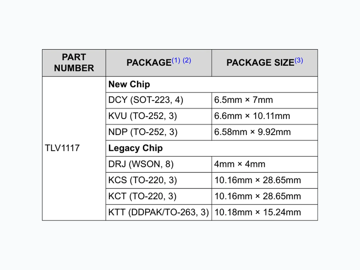
NUMBER PACKAGE(1) (2) PACKAGE SIZE(3) TLV1117 New Chip DCY (SOT-223, 4) 6.5mm × 7mm KVU (TO-252, 3) 6.6mm × 10.11mm NDP (TO-252, 3) 6.58mm × 9.92mm Legacy Chip DRJ (WSON, 8) 4mm × 4mm KCS (TO-220, 3) 10.16mm × 28.65mm KCT (TO-220, 3) 10.16mm × 28.65mm KTT (DDPAK/TO-263, 3) 10.18mm × 15.24mm (1) For more information, see the Mechanical, Packaging, and Orderable Information. (2) For legacy and new chip details, see the Device Nomenclature section. (3) The package size (length × width) is a nominal value and includes pins, where applicable. TLV1117 SLVS561O – DECEMBER 2004 – REVISED JUNE 2025 An IMPORTANT NOTICE at the end of this data sheet addresses availability, warranty, changes, use in safety-critical applications, intellectual property matters and other important disclaimers. PRODUCTION DATA.
10 Mechanical, Packaging, and Orderable
SLVS561O – DECEMBER 2004 – REVISED JUNE 2025 www.ti.com
2 Submit Document Feedback Copyright © 2025 Texas Instruments Incorporated
Product Folder Links: TLV1117
4 Pin Configuration and Functions
Figure 4-1. DCY Package, 4-Pin SOT (Top View) ADJ/GND OUTPUT INPUT Figure 4-2. KCT and KCS Package, 3-Pin TO-220 (Top View) ADJ/GND OUTPUT INPUT OUTPUT Figure 4-3. KTT Package, 3-Pin TO-263 (Top View) ADJ/GND OUTPUT INPUT OUTPUT Figure 4-4. KVU Package, 3-Pin TO-252 (Top View) VOUT 4 5 8ADJ/GND VIN (1) VIN (1) VIN (1) NC VOUT (2) VOUT (2) VOUT (2) Figure 4-5. DRJ Package, 8-Pin WSON (Top View) Table 4-1. Pin Functions PIN TYPE DESCRIPTION NAME KTT KVU DCY DRJ KCT ADJ/GND 1 1 1 1 1 I/O Adjust pin for adjustable output option. Ground pin for fixed output option. INPUT (VIN) 3 3 3 2, 3, 4 3 I Input voltage pin for the regulator. For the DRJ package, connect the VIN and VOUT pins together. OUTPUT (VOUT) 2 2 2 5, 6, 7 2 O Output voltage pin for the regulator. For the DRJ package, connect the VIN and VOUT pins together. NC — — — 8 — — No connect. www.ti.com TLV1117 SLVS561O – DECEMBER 2004 – REVISED JUNE 2025 Copyright © 2025 Texas Instruments Incorporated Submit Document Feedback 3 Product Folder Links: TLV1117
5 Specifications
5.1 Absolute Maximum Ratings
over operating free-air temperature range (unless otherwise noted)(1) MIN MAX UNIT VIN (2) Continuous input voltage –0.3 16 V VOUT (3) Output voltage (new chip, fixed version only) –0.3 VIN + 0.3 V Power Power dissipation Package limited (4) W Temperature Operating junction (Tj) –50 150 Storage (Tstg) –65 150 (1) Operation outside the Absolute Maximum Ratings may cause permanent device damage. Absolute Maximum Ratings do not imply functional operation of the device at these or any other conditions beyond those listed under Recommended Operating Conditions. If used outside the Recommended Operating Conditions but within the Absolute Maximum Ratings, the device may not be fully functional, and this may affect device reliability, functionality, performance, and shorten the device lifetime. (2) All voltages with respect to GND. (3) VIN + 0.3V or 16V (whichever is smaller). (4) See Thermal Information table for further details.
5.2 ESD Ratings
(Legacy Chip) VALUE (New Chip, Fixed Output) VALUE (New Chip, Adjustable Output) UNIT V(ESD) Electrostatic discharge Human body model (HBM), per ANSI/ESDA/ JEDEC JS-001, all pins(1) ±2500 ±3000 ±2000 V Charged device model (CDM), per JEDEC specification JESD22-C101, all pins(2) ±1500 ±1000 NA (1) JEDEC document JEP155 states that 500V HBM allows safe manufacturing with a standard ESD control process. (2) JEDEC document JEP157 states that 250V CDM allows safe manufacturing with a standard ESD control process. TLV1117 SLVS561O – DECEMBER 2004 – REVISED JUNE 2025 www.ti.com
4 Submit Document Feedback Copyright © 2025 Texas Instruments Incorporated
Product Folder Links: TLV1117
5.3 Recommended Operating Conditions
over operating free-air temperature range (unless otherwise noted) MIN NOM MAX UNIT VIN Input voltage TLV1117 2.7 15 V TLV1117-15 2.9 15 TLV1117-18 3.2 15 TLV1117-25 3.9 15 TLV1117-33 4.7 15 TLV1117-50 6.4 15 IOUT Output current 0.8 A COUT ESR (1) Output capacitor ESR (new chip, fixed output) 2 500 mΩ TJ (2) Junction temperature TLV1117C 0 125 TLV1117I –40 125 (1) Maximum supported ESR range for new chip, fixed output is 0.5Ω. For output capacitor with higher ESR values, place a low ESR MLCC capacitor. (2) The maximum power dissipation is a function of TJ(max) , RθJA, and TA. The maximum allowable power dissipation at any ambient temperature is PD = (TJ(max)–TA) / RθJA. All numbers apply for packages soldered directly into a PCB. www.ti.com TLV1117 SLVS561O – DECEMBER 2004 – REVISED JUNE 2025 Copyright © 2025 Texas Instruments Incorporated Submit Document Feedback 5 Product Folder Links: TLV1117
5.4 Thermal Information (Legacy Chip)
THERMAL METRIC(1) Legacy chip (2) UNITKTE (PowerFlex) KTP (PowerFlex) DRJ DCY KVU KCS, KCT KTT
3 PINS 3 PINS 8 PINS 4 PINS 3 PINS 3 PINS 3 PINS
RθJA Junction-to-ambient thermal Rθ JC(top) Junction-to-case (top) thermal RθJB Junction-to-board thermal ΨJT Junction-to-top ΨJB Junction-to-board Rθ JC(bot) Junction-to-case (bottom) thermal resistance 3 3 4.7 n/a 0.4 0.4 0.3 °C/W RθJP Thermal resistance between the die junction and the bottom of the exposed pad. 2.7 1.4 1.78 n/a n/a 3 1.94 °C/W (1) For more information about traditional and new thermal metrics, see the Semiconductor and IC Package Thermal Metrics application note. (2) For thermal estimates of this device based on PCB copper area, see the TI PCB Thermal Calculator.
5.5 Thermal Information (New Chip)
THERMAL METRIC (1) Fixed Output Adjustable Output UNITDCY (SOT–223) KVU (TO-252) DCY (SOT–223) KVU (TO–252)
4 PINS 4 PINS 4 PINS 4 PINS
RθJA Junction-to-ambient thermal resistance 95.4 67.2 61.6 45.1 °C/W RθJC(top) Junction-to-case (top) thermal resistance 55.6 71.8 42.5 52.1 °C/W RθJB Junction-to-board thermal resistance 33.7 45.5 10.4 29.8 °C/W ΨJT Junction-to-top characterization parameter 13.9 31.6 2.9 4.5 °C/W ΨJB Junction-to-board characterization parameter 33.4 45.4 10.3 29.4 °C/W RθJC(bot) Junction-to-case (bottom) thermal resistance N/A 40.5 N/A 1.3 °C/W (1) For more information about traditional and new thermal metrics, see the Semiconductor and IC Package Thermal Metrics application note. TLV1117 SLVS561O – DECEMBER 2004 – REVISED JUNE 2025 www.ti.com
6 Submit Document Feedback Copyright © 2025 Texas Instruments Incorporated
Product Folder Links: TLV1117
5.6 Electrical Characteristics
TJ = –40°C to 125°C for I version, TJ = 0°C to 125°C for C version, and all typical values are at TJ = 25°C (unless otherwise noted) PARAMETER (1) TEST CONDITIONS(10) MIN (4) TYP (5) MAX (4) UNIT VREF Reference voltage VIN – VOUT = 2V, IOUT = 10mA, TJ = 25℃ TLV1117C/I 1.238 1.25 1.262 V VIN – VOUT = 1.4V to 10V, IOUT = 10mA to 800mA TLV1117C 1.225 1.25 1.27 TLV1117I 1.2 1.25 1.29 VOUT Output voltage VIN = 3.5V, IOUT = 10mA, TJ = 25°C TLV1117C/I-15 1.485 1.5 1.515 V VIN = 2.9V to 10V, IOUT = 0mA to 800mA TLV1117C-15 1.455 1.5 1.545 TLV1117I-15 1.44 1.5 1.56 VIN = 3.8V, IOUT = 10mA, TJ = 25°C TLV1117C/I-18 1.782 1.8 1.818 VIN = 3.2V to 10V, IOUT = 0mA to 800mA TLV1117C-18 1.746 1.8 1.854 TLV1117I-18 1.728 1.8 1.872 VIN = 4.5V, IOUT = 10mA, TJ = 25°C TLV1117C/I-25 2.475 2.5 2.525 VIN = 3.9V to 10V, IOUT = 0mA to 800mA TLV1117C-25 2.450 2.5 2.550 TLV1117I-25 2.4 2.5 2.6 VIN = 5V, IOUT = 10mA, TJ = 25°C TLV1117C/I-33 3.267 3.3 3.333 VIN = 4.75V to 10V, IOUT = 0mA to 800mA TLV1117C-33 3.235 3.3 3.365 TLV1117I-33 3.168 3.3 3.432 VIN = 7V, IOUT = 10mA, TJ = 25°C TLV1117C/I-50 4.950 5.0 5.050 VIN = 6.5V to 12V, IOUT = 0mA to 800mA TLV1117C-50 4.900 5.0 5.1 TLV1117I-50 4.80 5.0 5.20 ΔVOUT(ΔVIN) Line regulation IOUT = 10mA, VIN – VOUT = 1.5V to 13.75V TLV1117C 0.035 0.2 TLV1117I 0.035 0.3 IOUT = 0mA, VIN = 2.9V to 10V TLV1117C-15 1 6 mV TLV1117I-15 1 10 mV IOUT = 0mA, VIN = 3.2V to 10V TLV1117C-18 1 6 TLV1117I-18 1 10 IOUT = 0mA, VIN = 3.9V to 10V TLV1117C-25 1 6 TLV1117I-25 1 10 IOUT = 0mA, VIN = 4.75V to 15V TLV1117C-33 1 6 TLV1117I-33 1 10 IOUT = 0mA, VIN = 6.5V to 15V TLV1117C-50 1 10 TLV1117I-50 1 15 ΔVOUT(ΔIOUT) Load regulation(6) IOUT = 0mA to 800mA, VIN = 2.9V TLV1117C-15 1 10 mV TLV1117I-15 1 15 IOUT = 0mA to 800mA, VIN = 3.2V TLV1117C-18 1 10 TLV1117I-18 1 15 IOUT = 0mA to 800mA, VIN = 3.9V TLV1117C-25 1 10 TLV1117I-25 1 15 IOUT = 0mA to 800mA, VIN = 4.75V TLV1117C-33 1 10 TLV1117I-33 1 15 IOUT = 0mA to 800mA, VIN = 6.5V TLV1117C-50 1 15 TLV1117I-50 1 20 VIN – VOUT = 3V, 10mA ≤ IOUT ≤ 800mA, TJ = 25℃ TLV1117C/I 0.2 VIN – VOUT = 3V, 10mA ≤ IOUT ≤ 800mA TLV1117C 0.4 TLV1117I 0.5 Load regulation (new chip, fixed output) 0mA ≤ IOUT ≤ 800mA TLV1117C/I 0.5 %/A www.ti.com TLV1117 SLVS561O – DECEMBER 2004 – REVISED JUNE 2025 Copyright © 2025 Texas Instruments Incorporated Submit Document Feedback 7 Product Folder Links: TLV1117
5.6 Electrical Characteristics (continued)
TJ = –40°C to 125°C for I version, TJ = 0°C to 125°C for C version, and all typical values are at TJ = 25°C (unless otherwise noted) PARAMETER (1) TEST CONDITIONS(10) MIN (4) TYP (5) MAX (4) UNIT VDO Dropout voltage(2) IOUT = 100mA TLV1117C 1.1 1.2 V TLV1117I 1.1 1.3 IOUT = 500mA TLV1117C 1.15 1.25 TLV1117I 1.15 1.35 IOUT = 800mA TLV1117C 1.2 1.3 TLV1117I 1.2 1.4 Dropout voltage (new chip, fixed output) (8) IOUT = 100mA TLV1117C/I 0.2 0.4 IOUT = 500mA TLV1117C/I 0.5 0.8 IOUT = 800mA TLV1117C/I 0.8 1.2 ICL Output current limit (3) VIN – VOUT = 5V, TJ = 25℃ TLV1117C/I 0.8 1.2 1.6 AOutput current limit (new chip, fixed output) VOUT = 0.9 x VOUT(NOM) , VIN = VOUT(nom) + 1.5V or VIN = 4.3V (whichever is greater) 1.1 1.6 ISC Short-circuit current limit (new chip, fixed output) VOUT = 0V 150 250 350 mA IMIN(LOAD) (7) Minimum load current VIN = 15V TLV1117C/I 1.7 5 mA IQ Quiescent current (adjustable output) VIN ≤ 15V TLV1117C 5 10 mA TLV1117I 5 15 Quiescent current (legacy chip, fixed output) VIN ≤ 15V TLV1117C 5 10 Quiescent current (legacy chip, fixed output) TLV1117I 5 15 Quiescent current (new chip, fixed output) IOUT = 0mA, VIN = 15V TLV1117C/I 65 110 µA Thermal regulation TA = 25°C, 30ms pulse TLV1117C/I 0.01 0.1 %/W PSRR Ripple rejection fRIPPLE = 120Hz, VIN – VOUT = 3V, VRIPPLE = 1VPP TLV1117C/I 60 75 dB Ripple rejection (new chip, fixed output) fRIPPLE = 120Hz, VIN – VOUT = 3V, VRIPPLE = 1VPP TLV1117C/I 70 dB IADJ ADJ pin current (legacy chip) TLV1117C/I 80 120 µA ADJ pin current (new chip) TLV1117C/I 60 120 ΔIADJ Adjust pin current change VIN – VOUT = 1.4V to 10V, IOUT= 10mA to 800mA TLV1117C 0.2 5 µA VIN – VOUT = 1.4V to 10V, IOUT= 10mA to 800mA TLV1117I 0.2 10 Temperature stability TJ = Full range 0.5 % Long-term stability 1000 hours, no load, TA = 125℃ 0.3 % Vn RMS output noise (legacy chip) % of VOUT, f = 10Hz to 100kHz 0.003 %RMS output noise (new chip, adjustable output) % of VOUT, f = 10Hz to 10kHz 0.003 RMS output noise (new chip, fixed output) BW = 10Hz to 100kHz, VIN = 3.3V, VOUT = 0.8V, IOUT = 100mA 60 µVRMS IPULLDOWN Output pulldown current (new chip, fixed output) (9) VIN = 1.8V, VOUT = 2.5V 0.7 1.1 mA VUVLO+ UVLO threshold rising (new chip, fixed output) VIN rising 2.2 2.4 V VUVLO- UVLO threshold falling (new chip, fixed output) VIN falling 1.9 V VUVLO(HYS) UVLO hysteresis (new chip, fixed output) 130 mV TSD(shutdown) Thermal shutdown temperature (new chip, fixed output) Temperature increasing 180 °C TSD(reset) Thermal shutdown reset temperature (new chip, fixed output) Temperature falling 160 °C (1) For legacy chip only: all characteristics are measured with a 10μF capacitor across the input and a 10μF capacitor across the output. Pulse testing techniques are used to maintain the junction temperature as close to the ambient temperature as possible. TLV1117 SLVS561O – DECEMBER 2004 – REVISED JUNE 2025 www.ti.com
8 Submit Document Feedback Copyright © 2025 Texas Instruments Incorporated
Product Folder Links: TLV1117
(2) Dropout is defined as the VIN to VOUT differential at which VOUT drops 100mV below the value of VOUT, measured at VIN = VOUT(nom) + 1.5V. (3) Current limit test specified under recommended operating conditions. (4) For new chip, adjustable output only: all limits are specified by testing or statistical analysis. (5) For new chip, adjustable output only: typical values represent the most likely parametric normal. (6) For new chip, adjustable output only: load and line regulation are measured at constant junction room temperature. (7) The minimum output current required to maintain regulation. (8) VDO is measured with VIN = 95% x VOUT(nom) for fixed output devices. VDO is not measured for fixed output devices when VOUT < 2.5V. (9) IPULLDOWN is measured with VIN = 1.8V (lower than UVLO falling threshold, with LDO in disabled state) and 2.5V applied on VOUT externally. (10) If VOUT level is not captured with device name (TLV1117C/I) column, than that particular spec is valid for both adjustable and fixed output devices. www.ti.com TLV1117 SLVS561O – DECEMBER 2004 – REVISED JUNE 2025 Copyright © 2025 Texas Instruments Incorporated Submit Document Feedback 9 Product Folder Links: TLV1117
5.7 Typical Characteristics
−0.35 −0.3 −0.25 −0.2 −0.15 −0.1 −0.05 Temperature (/C0053C) 1251007550250−25−50 /C0068VOUT (%) /C0068Load = 800 mA Figure 5-1. Load Regulation (Legacy Chip) VIN ≥ 3.0V Figure 5-2. VOUT Accuracy vs IOUT (Fixed Output, New Chip) IOUT = 10mA Figure 5-3. VOUT Accuracy vs VIN (Fixed Output, New Chip) Figure 5-4. Load Regulation (Adjustable Output, New Chip) Input/Output Differential (V) Short-Circui t Current (A) 0.2 0.4 0.6 0.8 1.2 1.4 1.6 1.8 TJ = 25/C0053C TJ = 125/C0053C 0 1512963 Figure 5-5. Short-Circuit Current vs (VIN – VOUT) (Legacy Chip) VIN ≥ 3.0V Figure 5-6. Foldback Current Limit vs Temperature (Fixed Output, New Chip) TLV1117 SLVS561O – DECEMBER 2004 – REVISED JUNE 2025 www.ti.com
10 Submit Document Feedback Copyright © 2025 Texas Instruments Incorporated
Product Folder Links: TLV1117
5.7 Typical Characteristics (continued)
Figure 5-7. Foldback Current Limit vs Temperature (Fixed Output, New Chip) Figure 5-8. Short-Circuit Current (Adjustable Output, New Chip) Frequency (Hz) Ripple Rejection (dB) 100k10k1k10010 Figure 5-9. Ripple Rejection vs Frequency (Adjustable Output, Legacy Chip) 0 200 400 600 800 Load (mA) Ripple Rejection (dB) f = 120 Hz Figure 5-10. Ripple Rejection vs Load Current (Adjustable Output, Legacy Chip) VOUT = 1.8V, VIN = 3.3V Figure 5-11. Ripple Rejection vs Frequency (Fixed Output, New Chip) VOUT = 1.8V, IOUT = 0.55A Figure 5-12. Ripple Rejection vs Frequency (Fixed Output, New Chip) www.ti.com TLV1117 SLVS561O – DECEMBER 2004 – REVISED JUNE 2025 Copyright © 2025 Texas Instruments Incorporated Submit Document Feedback 11 Product Folder Links: TLV1117
Figure 5-13. Ripple Rejection vs Frequency (Adjustable Output, New Chip) Figure 5-14. Ripple Rejection vs Frequency (Adjustable Output, New Chip) −1.5 −0.5 0.5 1.5 Temperature (/C0053C) Output Voltage Variation (%) 1251007550250−25−50 150 Figure 5-15. Temperature Stability (Legacy Chip) Figure 5-16. Temperature Stability (Adjustable Output, New Chip) 100 110 120 130 140 150 Temperature (/C0053C) ADJ Pin Current (/C0109A) 1251007550250−25−50 150 Figure 5-17. ADJ Pin Current vs Temperature (Legacy Chip) Figure 5-18. ADJ Pin Current vs Temperature (New Chip) TLV1117 SLVS561O – DECEMBER 2004 – REVISED JUNE 2025 www.ti.com
12 Submit Document Feedback Copyright © 2025 Texas Instruments Incorporated
Product Folder Links: TLV1117
−0.5 −0.4 −0.3 −0.2 −0.1 0.1 0.2 Time (/C0109s) Output Voltage Deviation (V) −0.2 0.2 0.4 0.6 0.8 1.2 1.4 1.6 1.8 2.2 2.4 2.6 Load Current (A) −60 200−20−40 CIN = 10 /C0109F COUT = 10-/C0109F Tantalum VIN = 4.8 V Preload = 0.1 A Output-Voltage Deviation Load Current Figure 5-19. TLV1117-33 Load Transient Response (Legacy Chip) VIN = 5V, VOUT = 3.3V, ramp rate = 0.4A/µs Figure 5-20. IOUT Transient From 0mA to 100mA (Fixed Output, New Chip) VIN = 5V, VOUT = 3.3V, ramp rate = 0.5A/µs Figure 5-21. IOUT Transient From 1mA to 1A (Fixed Output, New Chip) VIN = 5V, VOUT = 3.3V, ramp rate = 0.8A/µs Figure 5-22. IOUT Transient From 250mA to 850mA (Fixed Output, New Chip) Figure 5-23. Load Transient Response (Adjustable Output, New Chip) −20 −10 100 Time (/C0109s) Output Voltage Deviation (mV) Input Voltage (V) CIN = 0.1 /C0109F COUT = 10-/C0109F Tantalum IOUT = 0.1 A −40 −20 0 20 40 60 80 100 120 140 Input Voltage Output-Voltage Deviation Figure 5-24. TLV1117-33 Line Transient Response (Legacy Chip) www.ti.com TLV1117 SLVS561O – DECEMBER 2004 – REVISED JUNE 2025 Copyright © 2025 Texas Instruments Incorporated Submit Document Feedback 13 Product Folder Links: TLV1117
VIN = 5V, VOUT = 3.3V, IOUT = 1A, VIN ramp rate = 0.6V/µs Figure 5-25. VIN Transient in Dropout From 4V to 13V (Fixed Output, New Chip) VOUT = 3.3V, IOUT = 33μA, VIN ramp rate = 1.6V/µs Figure 5-26. VIN Transient From 5V to 16V (Fixed Output, New Chip) Figure 5-27. Line Transient Response (Adjustable Output, New Chip) 0.2 0.4 0.6 0.8 1.2 1.4 Load Current (mA) Dropout Voltage (V) 0 800700600500400300200100 TJ = 25/C0053C TJ = 125/C0053C Figure 5-28. Dropout Voltage vs Load Current (Legacy Chip) VIN ≥ 3.0V Figure 5-29. Dropout Voltage vs Load Current (Fixed Output, New Chip) IOUT = 1.0A Figure 5-30. Dropout Voltage vs VIN (Fixed Output, New Chip) TLV1117 SLVS561O – DECEMBER 2004 – REVISED JUNE 2025 www.ti.com
14 Submit Document Feedback Copyright © 2025 Texas Instruments Incorporated
Product Folder Links: TLV1117
IOUT = 0.8A Figure 5-31. Dropout Voltage vs VIN (Fixed Output, New Chip) Figure 5-32. Dropout Voltage vs Load Current (Adjustable Output, New Chip) IOUT = 0mA Figure 5-33. IQ vs Temperature (Fixed Output, New Chip) IOUT = 0mA Figure 5-34. IQ Increase Below Minimum VIN (Fixed Output, New Chip) VIN ≥ 3.0V Figure 5-35. IGND vs IOUT (Fixed Output, New Chip) Figure 5-36. UVLO Thresholds vs Temperature (Fixed Output, New Chip) www.ti.com TLV1117 SLVS561O – DECEMBER 2004 – REVISED JUNE 2025 Copyright © 2025 Texas Instruments Incorporated Submit Document Feedback 15 Product Folder Links: TLV1117
IOUT = 0.1A, RMS noise BW = 10Hz to 100kHz Figure 5-37. Output Noise (Vn) vs VOUT (Fixed Output, New Chip) T i m e ( m s ) Voltage (V) Current (A) - 1 - 1 . 7 5 0 - 1 . 5 1 - 1 . 2 5 2 - 1 3 - 0 . 7 5 4 - 0 . 5 5 - 0 . 2 5 6 0 7 0 . 2 5 8 0 . 5 9 0 . 7 5 V I N I I N V O U T IOUT = 0.1A, COUT = 22µF Figure 5-38. Inrush Current With 22µF at COUT (Fixed Output, New Chip) TLV1117 SLVS561O – DECEMBER 2004 – REVISED JUNE 2025 www.ti.com
16 Submit Document Feedback Copyright © 2025 Texas Instruments Incorporated
Product Folder Links: TLV1117
6 Detailed Description
6.1 Overview
The TLV1117 is a positive low-dropout voltage regulator designed to provide up to 800mA of output current. The device is available in both fixed (1.5V to 5V), and adjustable (1.25V to 13.8V) output voltage configurations. For new chip configurations, all internal circuitry is designed to operate down to a 1.5V, input-to-output differential. Dropout voltage is specified at a maximum of 1.3V at 800mA, decreasing at lower load currents. The fixed version (new chip) features integrated foldback current limit, thermal shutdown, internal output pulldown, and undervoltage lockout (UVLO). The adjustable version (new chip) develops a 1.25V reference voltage (VREF) between the OUTPUT and the ADJ pin.
6.2 Functional Block Diagrams
1.25 V 80 /UNI21dA 5 mA INPUT OUTPUT ADJUST Overload Block Figure 6-1. Functional Block Diagram (Legacy Chip) Bandgap Reference VREF = 0.8 V VIN VOUT GND Internal Controller UVLO Current Limit Thermal Shutdown R1R2 GND Output Pull-down GND GND Figure 6-2. Functional Block Diagram (Fixed Output, New Chip) www.ti.com TLV1117 SLVS561O – DECEMBER 2004 – REVISED JUNE 2025 Copyright © 2025 Texas Instruments Incorporated Submit Document Feedback 17 Product Folder Links: TLV1117
Figure 6-3. Functional Block Diagram (Adjustable Output, New Chip)
6.3 Feature Description
6.3.1 Dropout Voltage (Fixed Output, New Chip)
Dropout voltage (V DO) is defined as V IN – V OUT at the rated output current (I RATED), where the pass transistor is fully on. V IN is the input voltage, V OUT is the output voltage, and I RATED is the maximum I OUT listed in the Recommended Operating Conditions table. At this operating point, the pass transistor is driven fully on. Dropout voltage indirectly specifies a minimum input voltage greater than the nominal programmed output voltage where the output voltage is expected to stay in regulation. If the input voltage falls to less than the nominal output regulation, then the output voltage falls as well. For a CMOS regulator, the dropout voltage is determined by the drain-source, on-state resistance (R DS(ON)) of the pass transistor. Therefore, if the linear regulator operates at less than the rated current, the dropout voltage for that current scales accordingly. The following equation calculates the RDS(ON) of the device. R =DS(ON) VDO IRA TED (1) TLV1117 SLVS561O – DECEMBER 2004 – REVISED JUNE 2025 www.ti.com
18 Submit Document Feedback Copyright © 2025 Texas Instruments Incorporated
Product Folder Links: TLV1117
6.3.2 Foldback Current Limit (Fixed Output, New Chip)
The device has an internal current limit circuit that protects the regulator during transient high-load current faults or shorting events. The current limit is a hybrid brick-wall-foldback scheme. The current limit transitions from a brick-wall scheme to a foldback scheme at the foldback voltage (V FOLDBACK). In a high-load current fault with the output voltage above V FOLDBACK, the brick-wall scheme limits the output current to the current limit (I CL). When the voltage drops below V FOLDBACK, a foldback current limit activates that scales back the current when the output voltage approaches GND. When the output is shorted, the device supplies a typical current termed the short-circuit current limit (ISC). ICL and ISC are listed in the Electrical Characteristics table. For this device, VFOLDBACK = 50% × VOUT(nom). The output voltage is not regulated when the device is in current limit. When a current limit event occurs, the device begins to heat up because of the increase in power dissipation. When the device is in brick-wall current limit, the pass transistor dissipates power [(V IN – VOUT) × ICL]. When the device output is shorted and the output is below V FOLDBACK, the pass transistor dissipates power [(V IN – V OUT) × I SC]. If thermal shutdown is triggered, the device turns off. After the device cools down, the internal thermal shutdown circuit turns the device back on. If the output current fault condition continues, the device cycles between current limit and thermal shutdown. For more information on current limits, see the Know Your Limits application note. Figure 6-4 shows a diagram of the foldback current limit. VOUT(NOM) 0 V 0 mA VOUT VFOLDBACK ICLISC IRATED IOUT Brickwall Foldback Figure 6-4. Foldback Current Limit
6.3.3 Undervoltage Lockout (Fixed Output, New Chip)
The device has an independent undervoltage lockout (UVLO) circuit that monitors the input voltage. This circuit allows for a controlled and consistent turn on and off of the output voltage. To prevent the device from turning off if the input drops during turn on, the UVLO has hysteresis as specified in the Electrical Characteristics table. www.ti.com TLV1117 SLVS561O – DECEMBER 2004 – REVISED JUNE 2025 Copyright © 2025 Texas Instruments Incorporated Submit Document Feedback 19 Product Folder Links: TLV1117
6.3.4 Thermal Shutdown (Fixed Output, New Chip)
The device contains a thermal shutdown protection circuit to disable the device when the junction temperature (TJ) of the pass transistor rises to T SD(shutdown) (typical). Thermal shutdown hysteresis makes sure that the device resets (turns on) when the temperature falls to TSD(reset) (typical). The thermal time-constant of the semiconductor die is fairly short. Thus the device cycles on and off when thermal shutdown is reached until power dissipation is reduced. Power dissipation during start-up is high from large VIN – VOUT voltage drops across the device or from high inrush currents charging large output capacitors. Under some conditions, the thermal shutdown protection disables the device before start-up completes. For reliable operation, limit the junction temperature to the maximum listed in the Recommended Operating Conditions table. Operation above this maximum temperature causes the device to exceed operational specifications. Although the device internal protection circuitry is designed to protect against thermal overload conditions, this circuitry is not intended to replace proper heat sinking. Continuously running the device into thermal shutdown or above the maximum recommended junction temperature reduces long-term reliability.
6.3.5 Load Regulation (Adjustable Output, New Chip)
The TLV1117 regulates the voltage that appears between the output and adjust pins. In some cases, line resistances introduce errors to the voltage across the load. To obtain the best load regulation, a few precautions are needed. Figure 6-5 shows a diagram using the adjustable regulator. Best performance is obtained with the positive side of resistor R1 tied directly to the regulator output terminal rather than near the load. This layout eliminates line drops from appearing effectively in series with the reference and degrading regulation. For example, a 5V regulator with 0.05 Ω resistance between the regulator and load has load regulation resulting from the line resistance of 0.05Ω × IL. If R1 (equal to 125 Ω) is connected near the load, the effective line resistance is 0.05 Ω × (1 + R2 / R1). In this case, the effective line resistance is four times worse. In addition, the ground side of the resistor R2 is returned near the ground of the load to provide remote ground sensing and improve load regulation. TLV1117-ADJ Figure 6-5. Best Load Regulation Using Adjustable Output Regulator TLV1117 SLVS561O – DECEMBER 2004 – REVISED JUNE 2025 www.ti.com
20 Submit Document Feedback Copyright © 2025 Texas Instruments Incorporated
Product Folder Links: TLV1117
6.4 Device Functional Modes
6.4.1 Device Functional Mode Comparison (Fixed Output, New Chip)
Table 6-1 shows the conditions that lead to the different modes of operation. See the Electrical Characteristics table for parameter values. Table 6-1. Device Functional Mode Comparison OPERATING MODE PARAMETER VIN IOUT TJ Normal operation VIN > VOUT(nom) + VDO and VIN > VIN(min) IOUT < IOUT(max) TJ < TSD(shutdown) Dropout operation VIN(min) < VIN < VOUT(nom) + VDO IOUT < IOUT(max) TJ < TSD(shutdown)
6.4.2 Normal Operation (Fixed Output)
The device regulates to the nominal output voltage when the following conditions are met: For the new chip:
- The input voltage is greater than the nominal output voltage plus the dropout voltage (VOUT(nom) + VDO)
- The output current is less than the current limit (IOUT < ICL)
- The device junction temperature is less than the thermal shutdown temperature (TJ < TSD) For the legacy chip:
- The device passes the bias current to the OUT pin. The load or feedback consumes the minimum load current captured in the Electrical Characteristics for regulation or the output is potentially too high.
6.4.3 Dropout Operation (Fixed Output, New Chip)
If the input voltage is lower than the nominal output voltage plus the specified dropout voltage, the device operates in dropout mode. In this mode, the output voltage tracks the input voltage. In this mode, the transient performance of the device becomes significantly degraded. During this mode, the pass transistor is driven fully on. Line or load transients in dropout potentially result in large output voltage deviations. When the device is in a steady dropout state, the pass transistor is driven fully on. This state is defined as when the device is in dropout, directly after being in a normal regulation state, but not during start-up. Dropout occurs when VIN < VOUT(NOM) + VDO. When the regulator exits dropout, the input voltage returns to a value ≥VOUT(NOM) + VDO. During this time, the output voltage potentially overshoots for a short period of time. V OUT(NOM) is the nominal output voltage and V DO is the dropout voltage. During dropout exit, the device pulls the pass transistor back from being driven fully on.
6.4.4 Protection Diodes (Adjustable Output, New Chip)
Under normal operation, the TLV1117 regulators do not need protection diodes. With the adjustable device, the internal resistance between the ADJ and output terminals limits the current. No diode is needed to divert the current around the regulator even with the capacitor on the ADJ terminal. The ADJ pin withstands a transient signal of ±25V with respect to the output voltage without damaging the device. When an output capacitor is connected to a regulator and the input is shorted to ground, the output capacitor discharges into the regulator output. The discharge current depends on the value of the capacitor, the output voltage of the regulator, and rate of decrease of V IN. In the TLV1117 regulators, the internal diode between the output and input pins withstands microsecond surge currents of 10A to 20A. With an extremely large output capacitor (≥1000µF), and with the input instantaneously shorted to ground, the regulator is potentially damaged. www.ti.com TLV1117 SLVS561O – DECEMBER 2004 – REVISED JUNE 2025 Copyright © 2025 Texas Instruments Incorporated Submit Document Feedback 21 Product Folder Links: TLV1117
In this case, as shown in Figure 6-6, place an external diode between the output and input pins to protect the regulator. TLV1117-ADJ Figure 6-6. Regulator With Protection Diode TLV1117 SLVS561O – DECEMBER 2004 – REVISED JUNE 2025 www.ti.com
22 Submit Document Feedback Copyright © 2025 Texas Instruments Incorporated
Product Folder Links: TLV1117
7 Application and Implementation
Information in the following applications sections is not part of the TI component specification, and TI does not warrant its accuracy or completeness. TI’s customers are responsible for determining suitability of components for their purposes, as well as validating and testing their design implementation to confirm system functionality.
7.1 Application Information
The TLV1117 is a versatile and high-performance, linear regulator with a wide temperature range and tight line and load regulation operation. An output capacitor is required to further improve transient response and stability. For the adjustable option, the ADJ pin can also be bypassed to achieve very-high, ripple-rejection ratios. The TLV1117 is versatile in the device applications, including being used as a post regulator for DC/DC converters, battery chargers, and microprocessor supplies.
7.1.1 Recommended Capacitor Types (Fixed Output, New Chip)
The device is designed to be stable using low equivalent series resistance (ESR) ceramic capacitors at the input and output. Multilayer ceramic capacitors have become the industry standard for these types of applications and are recommended, but use good judgment. Ceramic capacitors that employ X7R-, X5R-, and C0G-rated dielectric materials provide relatively good capacitive stability across temperature. However, using Y5V-rated capacitors is discouraged because of large variations in capacitance. Regardless of the ceramic capacitor type selected, the effective capacitance varies with operating voltage and temperature. Generally, expect the effective capacitance to decrease by as much as 50%. The input and output capacitors listed in the Recommended Operating Conditions table account for an effective capacitance of approximately 50% of the nominal value.
7.1.2 Input and Output Capacitor Requirements (Fixed Output, New Chip)
Although an input capacitor is not required for stability, good analog design practice is to connect a capacitor from IN to GND. This capacitor counteracts reactive input sources and improves transient response, input ripple, and PSRR. Use an input capacitor if the source impedance is more than 0.5 Ω. Use a higher value capacitor if large, fast rise-time, load, or line transients are anticipated. Additionally, use a higher-value capacitor if the device is located several inches from the input power source. Dynamic performance of the device is improved by using an output capacitor. Use an output capacitor within the range specified in the Recommended Operating Conditions table for stability.
7.1.3 Reverse Current (Fixed Output, New Chip)
Excessive reverse current potentially damages this device. Reverse current flows through the intrinsic body diode of the pass transistor instead of the normal conducting channel. At high magnitudes, this current flow degrades the long-term reliability of the device. Conditions where reverse current occur are outlined in this section, all of which potentially exceed the absolute maximum rating of VOUT ≤ VIN + 0.3V.
- If the device has a large COUT and the input supply collapses with little or no load current
- The output is biased when the input supply is not established
- The output is biased above the input supply If reverse current flow is expected in the application, use external protection to protect the device. Reverse current is not limited in the device, so external limiting is required if extended reverse voltage operation is anticipated. www.ti.com TLV1117 SLVS561O – DECEMBER 2004 – REVISED JUNE 2025 Copyright © 2025 Texas Instruments Incorporated Submit Document Feedback 23 Product Folder Links: TLV1117
Figure 7-1 shows one approach for protecting the device. Device IN OUT GND COUT CIN Schottky Diode Internal Body Diode Figure 7-1. Example Circuit for Reverse Current Protection Using a Schottky Diode
7.1.4 Power Dissipation (Fixed Output, New Chip)
Circuit reliability requires proper consideration pf the device power dissipation, location of the circuit on the printed circuit board (PCB), and correct sizing of the thermal plane. Make sure the PCB area around the regulator has few or no other heat-generating devices that cause added thermal stress. To first-order approximation, power dissipation in the regulator depends on the input-to-output voltage difference and load conditions. The following equation calculates power dissipation (PD). PD = (VIN – VOUT) × IOUT (2) Note Power dissipation is minimized, and therefore greater efficiency achieved, by correct selection of the system voltage rails. For the lowest power dissipation, use the minimum input voltage required for correct output regulation. For devices with a thermal pad, the primary heat conduction path for the device package is through the thermal pad to the PCB. Solder the thermal pad to a copper pad area under the device. Make sure this pad area contains an array of plated vias that conduct heat to additional copper planes for increased heat dissipation. The maximum power dissipation determines the maximum allowable ambient temperature (T A) for the device. According to the following equation, power dissipation and junction temperature are most often related by the junction-to-ambient thermal resistance (R θJA) of the combined PCB and device package and the temperature of the ambient air (TA). The maximum power dissipation determines the maximum allowable ambient temperature (T A) for the device. Power dissipation and junction temperature are most often related by the R θJA of the combined PCB and device package and the TA. RθJA is the junction-to-ambient thermal resistance and TA is the temperature of the ambient air. The following equation describes this relationship. TJ = TA + (RθJA × PD) (3) Thermal resistance (R θJA) is highly dependent on the heat-spreading capability built into the particular PCB design. This resistance therefore varies according to the total copper area, copper weight, and location of the planes. The junction-to-ambient thermal resistance listed in the Thermal Information table is determined by the JEDEC standard PCB and copper-spreading area. R θJA is used as a relative measure of package thermal performance. TLV1117 SLVS561O – DECEMBER 2004 – REVISED JUNE 2025 www.ti.com
24 Submit Document Feedback Copyright © 2025 Texas Instruments Incorporated
Product Folder Links: TLV1117
7.1.5 Estimating Junction Temperature (Fixed Output, New Chip)
The JEDEC standard now recommends using psi ( Ψ) thermal metrics to estimate the linear regulator junction temperatures when in-circuit on a typical PCB board application. These metrics are not thermal resistance parameters and instead offer a practical and relative way to estimate junction temperature. These psi metrics are determined to be significantly independent of the copper area available for heat-spreading. The Thermal Information table lists the primary thermal metrics, which are the junction-to-top characterization parameter ( ψJT) and junction-to-board characterization parameter ( ψJB). These parameters provide two methods for calculating the junction temperature (T J), as described in the following equations. Use the junction-to-top characterization parameter ( ψJT) with the temperature at the center-top of device package (T T) to calculate the junction temperature. Use the junction-to-board characterization parameter ( ψJB) with the printed circuit board (PCB) surface temperature 1mm from the device package (TB) to calculate the junction temperature. TJ = TT + ψJT × PD (4) where:
- PD is the dissipated power
- TT is the temperature at the center-top of the device package TJ = TB + ψJB × PD (5) where:
- TB is the PCB surface temperature measured 1mm from the device package and centered on the package edge For detailed information on the thermal metrics and how to use the metrics, see the Semiconductor and IC Package Thermal Metrics application note.
7.2 Typical Application (Adjustable Output)
10 µF (see Note C) 100 µF (see Note A) INPUT OUTPUT ADJ/GND TLV1117 − ADJ VOVI CADJ (see Note B) 1N4002 (See Note D) IADJ VREF Figure 7-2. Basic Adjustable Regulator Note The Design Requirements (Adjustable Output) section lists details for notes referenced in Figure 7-2. The adjustable version of the TLV1117 takes a 2.7V to 15V input. The VREF voltage refers to the voltage between the output and the ADJUST pin, typically 1.25V. The V REF voltage causes current to flow across R1, which is the same current that flows across R2 (minus the negligible 50µA I ADJ). Therefore, adjust R2 to create a larger www.ti.com TLV1117 SLVS561O – DECEMBER 2004 – REVISED JUNE 2025 Copyright © 2025 Texas Instruments Incorporated Submit Document Feedback 25 Product Folder Links: TLV1117
voltage drop from GND and set the output voltage. The output voltage equation is described in the Detailed Design Procedure (Adjustable Output) section.
7.2.1 Design Requirements (Adjustable Output)
The bullets in this section are in reference to Figure 7-2.
- Note A: Output capacitor selection is critical for regulator stability. Larger COUT values benefit the regulator by improving transient response and loop stability. This device is designed to be stable with tantalum and aluminum electrolytic output capacitors with an ESR between 0.2Ω and 10Ω.
- Note B: Use CADJ to improve ripple rejection. If CADJ is used, a make sure to use a COUT that is larger in value than CADJ.
- Note C: Use CIN if the TLV1117 is not located near the power-supply filter.
- Note D: Use an external diode to protect the regulator if the input is instantaneously shorted to GND.
7.2.2 Detailed Design Procedure
7.2.2.1 Detailed Design Procedure (Fixed Output, New Chip)
For this design example, the 3.3V, fixed-version TLV1117-3.3 is selected and is powered by a standard 12V input supply. Keep the dropout voltage (V DO) within the TLV1117-3.3 dropout voltage specification for the 3.3V output voltage option. This voltage level keeps the device in regulation under all load and temperature conditions for this design. Use a 1.0µF output capacitor for excellent load transient response. The input capacitor is optional and is used to reduce the input impedance of the circuit and improve the transient response. As with any regulator, increasing the size of the output capacitor reduces overshoot and undershoot magnitude.
7.2.2.2 Detailed Design Procedure (Adjustable Output)
Calculate the output voltage with the following equation: V O U T = V RE F × 1 + R 2 R 1 + I A D J × R 2 (6) Neglecting I ADJ is permissible in most applications because the value is approximately 50 μA (new chip) and 80μA (legacy chip). TLV1117 SLVS561O – DECEMBER 2004 – REVISED JUNE 2025 www.ti.com
26 Submit Document Feedback Copyright © 2025 Texas Instruments Incorporated
Product Folder Links: TLV1117
7.2.3 Application Curves
0.2 0.4 0.6 0.8 1.2 1.4 Load Current (mA) Dropout Voltage (V) 0 800700600500400300200100 TJ = 25/C0053C TJ = 125/C0053C Figure 7-3. Dropout Voltage vs Load Current (Legacy Chip) Figure 7-4. Load Transient Response (Adjustable Output, New Chip) Figure 7-5. Line Transient Response (Adjustable Output, New Chip) VIN = 5V, VOUT = 3.3V, ramp rate = 0.4A/µs Figure 7-6. Load Transient Response, 1mA to 100mA (Fixed Output, New Chip) VIN = 5V, VOUT = 3.3V, ramp rate = 0.5A/µs Figure 7-7. Load Transient Response, 1mA to 1A (Fixed Output, New Chip) VIN = 5V, VOUT = 3.3V, ramp rate = 0.8A/µs Figure 7-8. Load Transient Response, 250mA to 850mA (Fixed Output, New Chip) www.ti.com TLV1117 SLVS561O – DECEMBER 2004 – REVISED JUNE 2025 Copyright © 2025 Texas Instruments Incorporated Submit Document Feedback 27 Product Folder Links: TLV1117
7.2.3 Application Curves (continued)
VIN = 5V, VOUT = 3.3V, IOUT = 1A, VIN ramp rate = 0.6V/µs Figure 7-9. Line Transient Response, 4V to 13V (Fixed Output, New Chip) VOUT = 3.3V, IOUT = 33μA, VIN ramp rate = 1.6V/µs Figure 7-10. Line Transient Response, 5V to 16V (Fixed Output, New Chip)
7.3 Power Supply Recommendations
The fixed and adjustable versions of the TLV1117 have different recommended ranges of operating voltage. See the Recommended Operating Conditions table for specific operating ranges.
7.4 Layout
7.4.1 Layout Guidelines
One or two input capacitors are recommended if the TLV1117 is not located near the power-supply output filter capacitor. These capacitors filter high-frequency noise and mitigate brief voltage surges from the input. Make sure traces on the device input and output pins are wide enough to support the full current range needed in the application to minimize I×R drop.
7.4.2 Layout Example
Figure 7-11. Layout Example TLV1117 SLVS561O – DECEMBER 2004 – REVISED JUNE 2025 www.ti.com
28 Submit Document Feedback Copyright © 2025 Texas Instruments Incorporated
Product Folder Links: TLV1117
8 Device and Documentation Support
8.1 Device Support
8.1.1 Device Nomenclature
Table 8-1. Available Options PRODUCT(1) (2) VOUT TLV1117-aaxyyyz Legacy chip aa is the nominal output voltage (for example 33 = 3.3V). x is the operating temperature range. yyy is the package designator. z is the package quantity.Fab source on the packaging label, CSO: SFB. TLV1117-aaxyyyz New chip aa is the nominal output voltage (for example 33 = 3.3V). x is the operating temperature range. yyy is the package designator. z is the package quantity.Fab source on the packaging label, CSO: RFB or CSO: FFAB. (1) Because this device ships with either legacy or new silicon, the product is identified with the fab source on the packaging label. (CSO: RFB, CSO: FFAB = new chip; CSO: SFB = legacy chip). Performance associated with the new and legacy chip is distinguished as such throughout the document. (2) For the most current package and ordering information, see the Package Option Addendum at the end of this document, or visit the device product folder at www.ti.com.
8.2 Receiving Notification of Documentation Updates
To receive notification of documentation updates, navigate to the device product folder on ti.com. Click on Notifications to register and receive a weekly digest of any product information that has changed. For change details, review the revision history included in any revised document.
8.3 Support Resources
TI E2E™ support forums are an engineer's go-to source for fast, verified answers and design help — straight from the experts. Search existing answers or ask your own question to get the quick design help you need. Linked content is provided "AS IS" by the respective contributors. They do not constitute TI specifications and do not necessarily reflect TI's views; see TI's Terms of Use.
8.4 Trademarks
TI E2E™ is a trademark of Texas Instruments. All trademarks are the property of their respective owners.
8.5 Electrostatic Discharge Caution
This integrated circuit can be damaged by ESD. Texas Instruments recommends that all integrated circuits be handled with appropriate precautions. Failure to observe proper handling and installation procedures can cause damage. ESD damage can range from subtle performance degradation to complete device failure. Precision integrated circuits may be more susceptible to damage because very small parametric changes could cause the device not to meet its published specifications.
8.6 Glossary
TI Glossary This glossary lists and explains terms, acronyms, and definitions.
9 Revision History
NOTE: Page numbers for previous revisions may differ from page numbers in the current version. Changes from Revision N (April 2025) to Revision O (June 2025) Page
- Updated Electrical Characteristics table to highlight performance sameness between legacy and new chip....7 www.ti.com TLV1117 SLVS561O – DECEMBER 2004 – REVISED JUNE 2025 Copyright © 2025 Texas Instruments Incorporated Submit Document Feedback 29 Product Folder Links: TLV1117
Changes from Revision M (January 2023) to Revision N (April 2025) Page
- Changed entire document to identify the features and differences of the legacy chip and new chip and the
10 Mechanical, Packaging, and Orderable Information
The following pages include mechanical packaging and orderable information. This information is the most current data available for the designated devices. This data is subject to change without notice and revision of this document. For browser based versions of this data sheet, refer to the left hand navigation. TLV1117 SLVS561O – DECEMBER 2004 – REVISED JUNE 2025 www.ti.com
30 Submit Document Feedback Copyright © 2025 Texas Instruments Incorporated
Product Folder Links: TLV1117
www.ti.com 24-Mar-2026 PACKAGING INFORMATION Orderable part number Status (1) Material type (2) Package | Pins Package qty | Carrier RoHS (3) Lead finish/ Ball material (4) MSL rating/ Peak reflow (5) Op temp (°C) Part marking (6) TLV1117-15CDCY Active Production SOT-223 (DCY) | 4 80 | TUBE Yes SN Level-2-260C-1 YEAR 0 to 125 T2 TLV1117-15CDCY.A Active Production SOT-223 (DCY) | 4 80 | TUBE Yes SN Level-2-260C-1 YEAR -40 to 125 T2 TLV1117-15CDCYR Active Production SOT-223 (DCY) | 4 2500 | LARGE T&R Yes SN Level-2-260C-1 YEAR 0 to 125 T2 TLV1117-15CDCYR.A Active Production SOT-223 (DCY) | 4 2500 | LARGE T&R Yes SN Level-2-260C-1 YEAR -40 to 125 T2 TLV1117-15CDCYRG3 Active Production SOT-223 (DCY) | 4 2500 | LARGE T&R Yes SN Level-2-260C-1 YEAR 0 to 125 T2 TLV1117-15CDRJR Active Production SON (DRJ) | 8 3000 | LARGE T&R Yes NIPDAU Level-2-260C-1 YEAR 0 to 125 ZYH TLV1117-15CDRJR.A Active Production SON (DRJ) | 8 3000 | LARGE T&R Yes NIPDAU Level-2-260C-1 YEAR -40 to 125 ZYH TLV1117-15IDCY Active Production SOT-223 (DCY) | 4 80 | TUBE Yes SN Level-2-260C-1 YEAR -40 to 125 T3 TLV1117-15IDCY.A Active Production SOT-223 (DCY) | 4 80 | TUBE Yes SN Level-2-260C-1 YEAR -40 to 125 T3 TLV1117-15IDCYR Active Production SOT-223 (DCY) | 4 2500 | LARGE T&R Yes SN Level-2-260C-1 YEAR -40 to 125 T3 TLV1117-15IDCYR.A Active Production SOT-223 (DCY) | 4 2500 | LARGE T&R Yes SN Level-2-260C-1 YEAR -40 to 125 T3 TLV1117-15IKVURG3 Active Production TO-252 (KVU) | 3 2500 | LARGE T&R Yes SN Level-3-260C-168 HR -40 to 125 ZF15 TLV1117-15IKVURG3.A Active Production TO-252 (KVU) | 3 2500 | LARGE T&R Yes SN Level-3-260C-168 HR -40 to 125 ZF15 TLV1117-18CDCY Active Production SOT-223 (DCY) | 4 80 | TUBE Yes SN Level-2-260C-1 YEAR 0 to 125 T4 TLV1117-18CDCY.A Active Production SOT-223 (DCY) | 4 80 | TUBE Yes SN Level-2-260C-1 YEAR -40 to 125 T4 TLV1117-18CDCYR Active Production SOT-223 (DCY) | 4 2500 | LARGE T&R Yes SN Level-2-260C-1 YEAR 0 to 125 T4 TLV1117-18CDCYR.A Active Production SOT-223 (DCY) | 4 2500 | LARGE T&R Yes SN Level-2-260C-1 YEAR -40 to 125 T4 TLV1117-18CDCYRG3 Active Production SOT-223 (DCY) | 4 2500 | LARGE T&R Yes SN Level-2-260C-1 YEAR 0 to 125 T4 TLV1117-18CDRJR Active Production SON (DRJ) | 8 3000 | LARGE T&R Yes NIPDAU Level-2-260C-1 YEAR 0 to 125 ZYK TLV1117-18CDRJR.A Active Production SON (DRJ) | 8 3000 | LARGE T&R Yes NIPDAU Level-2-260C-1 YEAR -40 to 125 ZYK TLV1117-18CKVURG3 Active Production TO-252 (KVU) | 3 2500 | LARGE T&R Yes SN Level-3-260C-168 HR 0 to 125 ZE18 TLV1117-18CKVURG3.A Active Production TO-252 (KVU) | 3 2500 | LARGE T&R Yes SN Level-3-260C-168 HR -40 to 125 ZE18 TLV1117-18IDCY Active Production SOT-223 (DCY) | 4 80 | TUBE Yes SN Level-2-260C-1 YEAR -40 to 125 T5 TLV1117-18IDCY.A Active Production SOT-223 (DCY) | 4 80 | TUBE Yes SN Level-2-260C-1 YEAR -40 to 125 T5 TLV1117-18IDCYR Active Production SOT-223 (DCY) | 4 2500 | LARGE T&R Yes SN Level-2-260C-1 YEAR -40 to 125 T5 TLV1117-18IDCYR.A Active Production SOT-223 (DCY) | 4 2500 | LARGE T&R Yes SN Level-2-260C-1 YEAR -40 to 125 T5 TLV1117-18IDCYRG3 Active Production SOT-223 (DCY) | 4 2500 | LARGE T&R Yes SN Level-2-260C-1 YEAR -40 to 125 T5 TLV1117-18IDRJR Active Production SON (DRJ) | 8 1000 | LARGE T&R Yes NIPDAU Level-2-260C-1 YEAR -40 to 125 ZYL TLV1117-18IDRJR.A Active Production SON (DRJ) | 8 1000 | LARGE T&R Yes NIPDAU Level-2-260C-1 YEAR -40 to 125 ZYL Addendum-Page 1
www.ti.com 24-Mar-2026 Orderable part number Status (1) Material type (2) Package | Pins Package qty | Carrier RoHS (3) Lead finish/ Ball material (4) MSL rating/ Peak reflow (5) Op temp (°C) Part marking (6) TLV1117-18IKVURG3 Active Production TO-252 (KVU) | 3 2500 | LARGE T&R Yes SN Level-3-260C-168 HR -40 to 125 ZF18 TLV1117-18IKVURG3.A Active Production TO-252 (KVU) | 3 2500 | LARGE T&R Yes SN Level-3-260C-168 HR -40 to 125 ZF18 TLV1117-25CDCY Active Production SOT-223 (DCY) | 4 80 | TUBE Yes SN Level-2-260C-1 YEAR 0 to 125 T6 TLV1117-25CDCY.A Active Production SOT-223 (DCY) | 4 80 | TUBE Yes SN Level-2-260C-1 YEAR -40 to 125 T6 TLV1117-25CDCYR Active Production SOT-223 (DCY) | 4 2500 | LARGE T&R Yes SN Level-2-260C-1 YEAR 0 to 125 T6 TLV1117-25CDCYR.A Active Production SOT-223 (DCY) | 4 2500 | LARGE T&R Yes SN Level-2-260C-1 YEAR -40 to 125 T6 TLV1117-25CDCYRG3 Active Production SOT-223 (DCY) | 4 2500 | LARGE T&R Yes SN Level-2-260C-1 YEAR 0 to 125 T6 TLV1117-25CKVURG3 Active Production TO-252 (KVU) | 3 2500 | LARGE T&R Yes SN Level-3-260C-168 HR 0 to 125 ZE25 TLV1117-25CKVURG3.A Active Production TO-252 (KVU) | 3 2500 | LARGE T&R Yes SN Level-3-260C-168 HR -40 to 125 ZE25 TLV1117-25IDCY Active Production SOT-223 (DCY) | 4 80 | TUBE Yes SN Level-2-260C-1 YEAR -40 to 125 T8 TLV1117-25IDCY.A Active Production SOT-223 (DCY) | 4 80 | TUBE Yes SN Level-2-260C-1 YEAR -40 to 125 T8 TLV1117-25IDCYR Active Production SOT-223 (DCY) | 4 2500 | LARGE T&R Yes SN Level-2-260C-1 YEAR -40 to 125 T8 TLV1117-25IDCYR.A Active Production SOT-223 (DCY) | 4 2500 | LARGE T&R Yes SN Level-2-260C-1 YEAR -40 to 125 T8 TLV1117-25IDRJR Active Production SON (DRJ) | 8 3000 | LARGE T&R Yes NIPDAU Level-2-260C-1 YEAR -40 to 125 ZYN TLV1117-25IDRJR.A Active Production SON (DRJ) | 8 3000 | LARGE T&R Yes NIPDAU Level-2-260C-1 YEAR -40 to 125 ZYN TLV1117-33CDCY Active Production SOT-223 (DCY) | 4 80 | TUBE Yes SN Level-2-260C-1 YEAR 0 to 125 V3 TLV1117-33CDCY.A Active Production SOT-223 (DCY) | 4 80 | TUBE Yes SN Level-2-260C-1 YEAR -40 to 125 V3 TLV1117-33CDCYG3 Active Production SOT-223 (DCY) | 4 80 | TUBE Yes SN Level-2-260C-1 YEAR 0 to 125 V3 TLV1117-33CDCYR Active Production SOT-223 (DCY) | 4 2500 | LARGE T&R Yes SN Level-2-260C-1 YEAR 0 to 125 V3 TLV1117-33CDCYR.A Active Production SOT-223 (DCY) | 4 2500 | LARGE T&R Yes SN Level-2-260C-1 YEAR -40 to 125 V3 TLV1117-33CDCYRG3 Active Production SOT-223 (DCY) | 4 2500 | LARGE T&R Yes SN Level-2-260C-1 YEAR 0 to 125 V3 TLV1117-33CDRJR Active Production SON (DRJ) | 8 1000 | LARGE T&R Yes NIPDAU Level-2-260C-1 YEAR 0 to 125 ZYP TLV1117-33CDRJR.A Active Production SON (DRJ) | 8 1000 | LARGE T&R Yes NIPDAU Level-2-260C-1 YEAR -40 to 125 ZYP TLV1117-33CKVURG3 Active Production TO-252 (KVU) | 3 2500 | LARGE T&R Yes SN Level-3-260C-168 HR 0 to 125 ZE33 TLV1117-33CKVURG3.A Active Production TO-252 (KVU) | 3 2500 | LARGE T&R Yes SN Level-3-260C-168 HR -40 to 125 ZE33 TLV1117-33IDCY Active Production SOT-223 (DCY) | 4 80 | TUBE Yes SN Level-2-260C-1 YEAR -40 to 125 (V3, VS) TLV1117-33IDCY.A Active Production SOT-223 (DCY) | 4 80 | TUBE Yes SN Level-2-260C-1 YEAR -40 to 125 (V3, VS) TLV1117-33IDCYG3 Active Production SOT-223 (DCY) | 4 80 | TUBE Yes SN Level-2-260C-1 YEAR -40 to 125 (V3, VS) TLV1117-33IDCYR Active Production SOT-223 (DCY) | 4 2500 | LARGE T&R Yes SN Level-2-260C-1 YEAR -40 to 125 VS TLV1117-33IDCYR.A Active Production SOT-223 (DCY) | 4 2500 | LARGE T&R Yes SN Level-2-260C-1 YEAR -40 to 125 VS TLV1117-33IDCYRG3 Active Production SOT-223 (DCY) | 4 2500 | LARGE T&R Yes SN Level-2-260C-1 YEAR -40 to 125 VS Addendum-Page 2
www.ti.com 24-Mar-2026 Orderable part number Status (1) Material type (2) Package | Pins Package qty | Carrier RoHS (3) Lead finish/ Ball material (4) MSL rating/ Peak reflow (5) Op temp (°C) Part marking (6) TLV1117-33IDRJR Active Production SON (DRJ) | 8 1000 | LARGE T&R Yes NIPDAU Level-2-260C-1 YEAR -40 to 125 ZYR TLV1117-33IDRJR.A Active Production SON (DRJ) | 8 1000 | LARGE T&R Yes NIPDAU Level-2-260C-1 YEAR -40 to 125 ZYR TLV1117-33IKVURG3 Active Production TO-252 (KVU) | 3 2500 | LARGE T&R Yes SN Level-3-260C-168 HR -40 to 125 ZF33 TLV1117-33IKVURG3.A Active Production TO-252 (KVU) | 3 2500 | LARGE T&R Yes SN Level-3-260C-168 HR -40 to 125 ZF33 TLV1117-50CDCY Active Production SOT-223 (DCY) | 4 80 | TUBE Yes SN Level-2-260C-1 YEAR 0 to 125 VT TLV1117-50CDCY.A Active Production SOT-223 (DCY) | 4 80 | TUBE Yes SN Level-2-260C-1 YEAR 0 to 125 VT TLV1117-50CDCYG3 Active Production SOT-223 (DCY) | 4 80 | TUBE Yes SN Level-2-260C-1 YEAR 0 to 125 VT TLV1117-50CDCYR Active Production SOT-223 (DCY) | 4 2500 | LARGE T&R Yes SN Level-2-260C-1 YEAR 0 to 125 VT TLV1117-50CDCYR.A Active Production SOT-223 (DCY) | 4 2500 | LARGE T&R Yes SN Level-2-260C-1 YEAR 0 to 125 VT TLV1117-50CDCYRG3 Active Production SOT-223 (DCY) | 4 2500 | LARGE T&R Yes SN Level-2-260C-1 YEAR 0 to 125 VT TLV1117-50CDRJR Active Production SON (DRJ) | 8 3000 | LARGE T&R Yes NIPDAU Level-2-260C-1 YEAR 0 to 125 ZE50 TLV1117-50CDRJR.A Active Production SON (DRJ) | 8 3000 | LARGE T&R Yes NIPDAU Level-2-260C-1 YEAR 0 to 125 ZE50 TLV1117-50CKVURG3 Active Production TO-252 (KVU) | 3 2500 | LARGE T&R Yes SN Level-3-260C-168 HR 0 to 125 ZE50 TLV1117-50CKVURG3.A Active Production TO-252 (KVU) | 3 2500 | LARGE T&R Yes SN Level-3-260C-168 HR 0 to 125 ZE50 TLV1117-50IDCY Active Production SOT-223 (DCY) | 4 80 | TUBE Yes SN Level-2-260C-1 YEAR -40 to 125 VU TLV1117-50IDCY.A Active Production SOT-223 (DCY) | 4 80 | TUBE Yes SN Level-2-260C-1 YEAR -40 to 125 VU TLV1117-50IDCYR Active Production SOT-223 (DCY) | 4 2500 | LARGE T&R Yes SN Level-2-260C-1 YEAR -40 to 125 VU TLV1117-50IDCYR.A Active Production SOT-223 (DCY) | 4 2500 | LARGE T&R Yes SN Level-2-260C-1 YEAR -40 to 125 VU TLV1117-50IDCYRG3 Active Production SOT-223 (DCY) | 4 2500 | LARGE T&R Yes SN Level-2-260C-1 YEAR -40 to 125 VU TLV1117-50IDRJR NRND Production SON (DRJ) | 8 1000 | LARGE T&R Yes NIPDAU Level-2-260C-1 YEAR -40 to 125 ZF50 TLV1117-50IDRJR.A NRND Production SON (DRJ) | 8 1000 | LARGE T&R Yes NIPDAU Level-2-260C-1 YEAR -40 to 125 ZF50 TLV1117-50IDRJRG4 NRND Production SON (DRJ) | 8 1000 | LARGE T&R Yes NIPDAU Level-2-260C-1 YEAR -40 to 125 ZF50 TLV1117-50IKVURG3 Active Production TO-252 (KVU) | 3 2500 | LARGE T&R Yes SN Level-3-260C-168 HR -40 to 125 ZF50 TLV1117-50IKVURG3.A Active Production TO-252 (KVU) | 3 2500 | LARGE T&R Yes SN Level-3-260C-168 HR -40 to 125 ZF50 TLV1117CDCY Active Production SOT-223 (DCY) | 4 80 | TUBE Yes SN Level-2-260C-1 YEAR 0 to 125 V4 TLV1117CDCY.A Active Production SOT-223 (DCY) | 4 80 | TUBE Yes SN Level-2-260C-1 YEAR -40 to 125 V4 TLV1117CDCYG3 Active Production SOT-223 (DCY) | 4 80 | TUBE Yes SN Level-2-260C-1 YEAR 0 to 125 V4 TLV1117CDCYR Active Production SOT-223 (DCY) | 4 2500 | LARGE T&R Yes SN Level-2-260C-1 YEAR 0 to 125 V4 TLV1117CDCYR.A Active Production SOT-223 (DCY) | 4 2500 | LARGE T&R Yes SN Level-2-260C-1 YEAR -40 to 125 V4 TLV1117CDCYR.B Active Production SOT-223 (DCY) | 4 2500 | LARGE T&R Yes SN Level-2-260C-1 YEAR -40 to 125 V4 TLV1117CDCYRG3 Active Production SOT-223 (DCY) | 4 2500 | LARGE T&R Yes SN Level-2-260C-1 YEAR 0 to 125 V4 Addendum-Page 3
www.ti.com 24-Mar-2026 Orderable part number Status (1) Material type (2) Package | Pins Package qty | Carrier RoHS (3) Lead finish/ Ball material (4) MSL rating/ Peak reflow (5) Op temp (°C) Part marking (6) TLV1117CDRJR Active Production SON (DRJ) | 8 1000 | LARGE T&R Yes NIPDAU Level-2-260C-1 YEAR 0 to 125 ZYS TLV1117CDRJR.A Active Production SON (DRJ) | 8 1000 | LARGE T&R Yes NIPDAU Level-2-260C-1 YEAR -40 to 125 ZYS TLV1117CKCS Active Production TO-220 (KCS) | 3 50 | TUBE Yes SN N/A for Pkg Type 0 to 125 TLV1117C TLV1117CKCS.A Active Production TO-220 (KCS) | 3 50 | TUBE Yes SN N/A for Pkg Type -40 to 125 TLV1117C TLV1117CKTTR Active Production DDPAK/ TO-263 (KTT) | 3 500 | LARGE T&R Yes SN Level-3-245C-168 HR 0 to 125 TLV1117C TLV1117CKTTR.A Active Production DDPAK/ TO-263 (KTT) | 3 500 | LARGE T&R Yes SN Level-3-245C-168 HR -40 to 125 TLV1117C TLV1117CKTTRG3 Active Production DDPAK/ TO-263 (KTT) | 3 500 | LARGE T&R Yes SN Level-3-245C-168 HR 0 to 125 TLV1117C TLV1117CKVURG3 Active Production TO-252 (KVU) | 3 2500 | LARGE T&R Yes SN Level-3-260C-168 HR 0 to 125 TV1117 TLV1117CKVURG3.A Active Production TO-252 (KVU) | 3 2500 | LARGE T&R Yes SN Level-3-260C-168 HR -40 to 125 TV1117 TLV1117CKVURG3.B Active Production TO-252 (KVU) | 3 2500 | LARGE T&R Yes SN Level-3-260C-168 HR -40 to 125 TV1117 TLV1117IDCY Active Production SOT-223 (DCY) | 4 80 | TUBE Yes SN Level-2-260C-1 YEAR -40 to 125 V2 TLV1117IDCY.A Active Production SOT-223 (DCY) | 4 80 | TUBE Yes SN Level-2-260C-1 YEAR -40 to 125 V2 TLV1117IDCYG3 Active Production SOT-223 (DCY) | 4 80 | TUBE Yes SN Level-2-260C-1 YEAR -40 to 125 V2 TLV1117IDCYR Active Production SOT-223 (DCY) | 4 2500 | LARGE T&R Yes SN Level-2-260C-1 YEAR -40 to 125 V2 TLV1117IDCYR.A Active Production SOT-223 (DCY) | 4 2500 | LARGE T&R Yes SN Level-2-260C-1 YEAR -40 to 125 V2 TLV1117IDCYR.B Active Production SOT-223 (DCY) | 4 2500 | LARGE T&R Yes SN Level-2-260C-1 YEAR -40 to 125 V2 TLV1117IDCYRG3 Active Production SOT-223 (DCY) | 4 2500 | LARGE T&R Yes SN Level-2-260C-1 YEAR -40 to 125 V2 TLV1117IDRJR Active Production SON (DRJ) | 8 1000 | LARGE T&R Yes NIPDAU Level-2-260C-1 YEAR -40 to 125 ZYT TLV1117IDRJR.A Active Production SON (DRJ) | 8 1000 | LARGE T&R Yes NIPDAU Level-2-260C-1 YEAR -40 to 125 ZYT TLV1117IKCS Active Production TO-220 (KCS) | 3 50 | TUBE Yes SN N/A for Pkg Type -40 to 125 TLV1117I TLV1117IKCS.A Active Production TO-220 (KCS) | 3 50 | TUBE Yes SN N/A for Pkg Type -40 to 125 TLV1117I TLV1117IKCSE3 Active Production TO-220 (KCS) | 3 50 | TUBE Yes SN N/A for Pkg Type -40 to 125 TLV1117I TLV1117IKTTR Active Production DDPAK/ TO-263 (KTT) | 3 500 | LARGE T&R Yes SN Level-3-245C-168 HR -40 to 125 TLV1117I TLV1117IKTTR.A Active Production DDPAK/ TO-263 (KTT) | 3 500 | LARGE T&R Yes SN Level-3-245C-168 HR -40 to 125 TLV1117I TLV1117IKVURG3 Active Production TO-252 (KVU) | 3 2500 | LARGE T&R Yes SN Level-3-260C-168 HR -40 to 125 (TV1117, TY1117) TLV1117IKVURG3.A Active Production TO-252 (KVU) | 3 2500 | LARGE T&R Yes SN Level-3-260C-168 HR -40 to 125 (TV1117, TY1117) TLV1117IKVURG3.B Active Production TO-252 (KVU) | 3 2500 | LARGE T&R Yes SN Level-3-260C-168 HR -40 to 125 (TV1117, TY1117) Addendum-Page 4
www.ti.com 24-Mar-2026 (1) Status: For more details on status, see our product life cycle. (2) Material type: When designated, preproduction parts are prototypes/experimental devices, and are not yet approved or released for full production. Testing and final process, including without limitation quality assurance, reliability performance testing, and/or process qualification, may not yet be complete, and this item is subject to further changes or possible discontinuation. If available for ordering, purchases will be subject to an additional waiver at checkout, and are intended for early internal evaluation purposes only. These items are sold without warranties of any kind. (3) RoHS values: Yes, No, RoHS Exempt. See the TI RoHS Statement for additional information and value definition. (4) Lead finish/Ball material: Parts may have multiple material finish options. Finish options are separated by a vertical ruled line. Lead finish/Ball material values may wrap to two lines if the finish value exceeds the maximum column width. (5) MSL rating/Peak reflow: The moisture sensitivity level ratings and peak solder (reflow) temperatures. In the event that a part has multiple moisture sensitivity ratings, only the lowest level per JEDEC standards is shown. Refer to the shipping label for the actual reflow temperature that will be used to mount the part to the printed circuit board. (6) Part marking: There may be an additional marking, which relates to the logo, the lot trace code information, or the environmental category of the part. Multiple part markings will be inside parentheses. Only one part marking contained in parentheses and separated by a "~" will appear on a part. If a line is indented then it is a continuation of the previous line and the two combined represent the entire part marking for that device. Important Information and Disclaimer:The information provided on this page represents TI's knowledge and belief as of the date that it is provided. TI bases its knowledge and belief on information provided by third parties, and makes no representation or warranty as to the accuracy of such information. Efforts are underway to better integrate information from third parties. TI has taken and continues to take reasonable steps to provide representative and accurate information but may not have conducted destructive testing or chemical analysis on incoming materials and chemicals. TI and TI suppliers consider certain information to be proprietary, and thus CAS numbers and other limited information may not be available for release. In no event shall TI's liability arising out of such information exceed the total purchase price of the TI part(s) at issue in this document sold by TI to Customer on an annual basis. Addendum-Page 5
PACKAGE MATERIALS INFORMATION www.ti.com 10-Aug-2026 TAPE AND REEL INFORMATION Reel Width (W1) REEL DIMENSIONS A0B0K0WDimension designed to accommodate the component lengthDimension designed to accommodate the component thicknessOverall width of the carrier tapePitch between successive cavity centersDimension designed to accommodate the component width TAPE DIMENSIONSK0 P1B0WA0Cavity QUADRANT ASSIGNMENTS FOR PIN 1 ORIENTATION IN TAPE Pocket QuadrantsSprocket HolesQ1Q1Q2Q2Q3Q3Q4Q4User Direction of Feed P1ReelDiameter *All dimensions are nominal Device Package Type Package Drawing Pins SPQ Reel Diameter (mm) Reel Width W1 (mm) (mm) (mm) (mm) (mm) W (mm) Pin1 Quadrant Pack Materials-Page 1
PACKAGE MATERIALS INFORMATION www.ti.com 10-Aug-2026 Device Package Type Package Drawing Pins SPQ Reel Diameter (mm) Reel Width W1 (mm) (mm) (mm) (mm) (mm) W (mm) Pin1 Quadrant TLV1117CKTTR DDPAK/ TO-263 TLV1117IKTTR DDPAK/ TO-263 Pack Materials-Page 2
PACKAGE MATERIALS INFORMATION www.ti.com 10-Aug-2026 TAPE AND REEL BOX DIMENSIONS Width (mm) W LH *All dimensions are nominal Device Package Type Package Drawing Pins SPQ Length (mm) Width (mm) Height (mm) TLV1117-15CDCYR SOT-223 DCY 4 2500 340.0 340.0 38.0 TLV1117-15CDCYR SOT-223 DCY 4 2500 336.0 336.0 48.0 TLV1117-15CDRJR SON DRJ 8 3000 353.0 353.0 32.0 TLV1117-15IDCYR SOT-223 DCY 4 2500 340.0 340.0 38.0 TLV1117-15IDCYR SOT-223 DCY 4 2500 336.0 336.0 48.0 TLV1117-15IKVURG3 TO-252 KVU 3 2500 340.0 340.0 38.0 TLV1117-18CDCYR SOT-223 DCY 4 2500 336.0 336.0 48.0 TLV1117-18CDCYR SOT-223 DCY 4 2500 340.0 340.0 38.0 TLV1117-18CDRJR SON DRJ 8 3000 353.0 353.0 32.0 TLV1117-18CKVURG3 TO-252 KVU 3 2500 340.0 340.0 38.0 TLV1117-18IDCYR SOT-223 DCY 4 2500 340.0 340.0 38.0 TLV1117-18IDCYR SOT-223 DCY 4 2500 336.0 336.0 48.0 TLV1117-18IDRJR SON DRJ 8 1000 213.0 191.0 35.0 TLV1117-18IKVURG3 TO-252 KVU 3 2500 340.0 340.0 38.0 TLV1117-25CDCYR SOT-223 DCY 4 2500 340.0 340.0 38.0 TLV1117-25CDCYR SOT-223 DCY 4 2500 336.0 336.0 48.0 TLV1117-25CKVURG3 TO-252 KVU 3 2500 340.0 340.0 38.0 TLV1117-25IDCYR SOT-223 DCY 4 2500 336.0 336.0 48.0 Pack Materials-Page 3
PACKAGE MATERIALS INFORMATION www.ti.com 10-Aug-2026 Device Package Type Package Drawing Pins SPQ Length (mm) Width (mm) Height (mm) TLV1117-25IDCYR SOT-223 DCY 4 2500 340.0 340.0 38.0 TLV1117-25IDRJR SON DRJ 8 3000 353.0 353.0 32.0 TLV1117-33CDCYR SOT-223 DCY 4 2500 340.0 340.0 38.0 TLV1117-33CDCYR SOT-223 DCY 4 2500 336.0 336.0 48.0 TLV1117-33CDRJR SON DRJ 8 1000 213.0 191.0 35.0 TLV1117-33CKVURG3 TO-252 KVU 3 2500 340.0 340.0 38.0 TLV1117-33IDCYR SOT-223 DCY 4 2500 340.0 340.0 38.0 TLV1117-33IDCYR SOT-223 DCY 4 2500 336.0 336.0 48.0 TLV1117-33IDRJR SON DRJ 8 1000 213.0 191.0 35.0 TLV1117-33IKVURG3 TO-252 KVU 3 2500 340.0 340.0 38.0 TLV1117-50CDCYR SOT-223 DCY 4 2500 340.0 340.0 38.0 TLV1117-50CDCYR SOT-223 DCY 4 2500 336.0 336.0 48.0 TLV1117-50CDRJR SON DRJ 8 3000 353.0 353.0 32.0 TLV1117-50CKVURG3 TO-252 KVU 3 2500 340.0 340.0 38.0 TLV1117-50IDCYR SOT-223 DCY 4 2500 336.0 336.0 48.0 TLV1117-50IDCYR SOT-223 DCY 4 2500 340.0 340.0 38.0 TLV1117-50IDRJR SON DRJ 8 1000 213.0 191.0 35.0 TLV1117-50IKVURG3 TO-252 KVU 3 2500 340.0 340.0 38.0 TLV1117CDCYR SOT-223 DCY 4 2500 340.0 340.0 38.0 TLV1117CDCYR SOT-223 DCY 4 2500 336.0 336.0 48.0 TLV1117CDCYR SOT-223 DCY 4 2500 367.0 367.0 35.0 TLV1117CKTTR DDPAK/TO-263 KTT 3 500 340.0 340.0 38.0 TLV1117CKVURG3 TO-252 KVU 3 2500 340.0 340.0 38.0 TLV1117CKVURG3 TO-252 KVU 3 2500 356.0 356.0 35.0 TLV1117IDCYR SOT-223 DCY 4 2500 367.0 367.0 35.0 TLV1117IDCYR SOT-223 DCY 4 2500 340.0 340.0 38.0 TLV1117IDCYR SOT-223 DCY 4 2500 336.0 336.0 48.0 TLV1117IDRJR SON DRJ 8 1000 213.0 191.0 35.0 TLV1117IKTTR DDPAK/TO-263 KTT 3 500 340.0 340.0 38.0 TLV1117IKVURG3 TO-252 KVU 3 2500 356.0 356.0 35.0 TLV1117IKVURG3 TO-252 KVU 3 2500 340.0 340.0 38.0 Pack Materials-Page 4
PACKAGE MATERIALS INFORMATION www.ti.com 10-Aug-2026 TUBE L - Tube length T - Tube height W - Tube width B - Alignment groove width *All dimensions are nominal Device Package Name Package Type Pins SPQ L (mm) W (mm) T (µm) B (mm) TLV1117-15CDCY DCY SOT-223 4 80 559 8.6 500 3.6 TLV1117-15CDCY.A DCY SOT-223 4 80 559 8.6 500 3.6 TLV1117-15IDCY DCY SOT-223 4 80 559 8.6 500 3.6 TLV1117-15IDCY.A DCY SOT-223 4 80 559 8.6 500 3.6 TLV1117-18CDCY DCY SOT-223 4 80 559 8.6 500 3.6 TLV1117-18CDCY.A DCY SOT-223 4 80 559 8.6 500 3.6 TLV1117-18IDCY DCY SOT-223 4 80 559 8.6 500 3.6 TLV1117-18IDCY.A DCY SOT-223 4 80 559 8.6 500 3.6 TLV1117-25CDCY DCY SOT-223 4 80 559 8.6 500 3.6 TLV1117-25CDCY.A DCY SOT-223 4 80 559 8.6 500 3.6 TLV1117-25IDCY DCY SOT-223 4 80 559 8.6 500 3.6 TLV1117-25IDCY.A DCY SOT-223 4 80 559 8.6 500 3.6 TLV1117-33CDCY DCY SOT-223 4 80 559 8.6 500 3.6 TLV1117-33CDCY.A DCY SOT-223 4 80 559 8.6 500 3.6 TLV1117-33CDCYG3 DCY SOT-223 4 80 559 8.6 500 3.6 TLV1117-33IDCY DCY SOT-223 4 80 559 8.6 500 3.6 TLV1117-33IDCY.A DCY SOT-223 4 80 559 8.6 500 3.6 TLV1117-33IDCYG3 DCY SOT-223 4 80 559 8.6 500 3.6 TLV1117-50CDCY DCY SOT-223 4 80 559 8.6 500 3.6 TLV1117-50CDCY.A DCY SOT-223 4 80 559 8.6 500 3.6 TLV1117-50CDCYG3 DCY SOT-223 4 80 559 8.6 500 3.6 TLV1117-50IDCY DCY SOT-223 4 80 559 8.6 500 3.6 TLV1117-50IDCY.A DCY SOT-223 4 80 559 8.6 500 3.6 TLV1117CDCY DCY SOT-223 4 80 542.9 8.6 3606 2.67 TLV1117CDCY DCY SOT-223 4 80 559 8.6 500 3.6 TLV1117CDCY.A DCY SOT-223 4 80 559 8.6 500 3.6 TLV1117CDCY.A DCY SOT-223 4 80 542.9 8.6 3606 2.67 TLV1117CDCYG3 DCY SOT-223 4 80 542.9 8.6 3606 2.67 TLV1117CDCYG3 DCY SOT-223 4 80 559 8.6 500 3.6 Pack Materials-Page 5
PACKAGE MATERIALS INFORMATION www.ti.com 10-Aug-2026 Device Package Name Package Type Pins SPQ L (mm) W (mm) T (µm) B (mm) TLV1117CKCS KCS TO-220 3 50 532 34.1 700 9.6 TLV1117CKCS.A KCS TO-220 3 50 532 34.1 700 9.6 TLV1117IDCY DCY SOT-223 4 80 559 8.6 500 3.6 TLV1117IDCY DCY SOT-223 4 80 542.9 8.6 3606 2.67 TLV1117IDCY.A DCY SOT-223 4 80 542.9 8.6 3606 2.67 TLV1117IDCY.A DCY SOT-223 4 80 559 8.6 500 3.6 TLV1117IDCYG3 DCY SOT-223 4 80 559 8.6 500 3.6 TLV1117IDCYG3 DCY SOT-223 4 80 542.9 8.6 3606 2.67 TLV1117IKCS KCS TO-220 3 50 532 34.1 700 9.6 TLV1117IKCS.A KCS TO-220 3 50 532 34.1 700 9.6 TLV1117IKCSE3 KCS TO-220 3 50 532 34.1 700 9.6 Pack Materials-Page 6
MPDS094A – APRIL 2001 – REVISED JUNE 2002 POST OFFICE BOX 655303 • DALLAS, TEXAS 75265 DCY (R-PDSO-G4) PLASTIC SMALL-OUTLINE 4202506/B 06/2002 6,30 (0.248) 6,70 (0.264) 2,90 (0.114) 3,10 (0.122) 6,70 (0.264) 3,30 (0.130) 0,02 (0.0008) 0,10 (0.0040) 1,50 (0.059) 1,70 (0.067) 0,23 (0.009) 0,35 (0.014) 1 2 3 0,66 (0.026) 0,84 (0.033) 1,80 (0.071) MAX Seating Plane 0°–10° Gauge Plane 0,75 (0.030) MIN 0,25 (0.010) 0,08 (0.003) 0,10 (0.004) M 2,30 (0.091) NOTES: A. All linear dimensions are in millimeters (inches). B. This drawing is subject to change without notice. C. Body dimensions do not include mold flash or protrusion. D. Falls within JEDEC TO-261 Variation AA.
www.ti.com PACKAGE OUTLINE 9.25 9.05 6.5 6.1 2.9 2.6 10.36 9.96 13.12 12.70
3.9 MAX
3X 1.36 1.23 3X 0.90 0.77 ( 3.84) 5.08 2X 2.54 8.55 8.15 12.5 12.1 (6.3)
19.65 MAX
4.7 4.4 1.32 1.22 2.79 2.59 0.47 0.34 4222214/B 08/2018 TO-220 - 19.65 mm max heightKCS0003B TO-220 NOTES: 1. Dimensions are in millimeters. Any dimension in brackets or parenthesis are for reference only. Dimensioning and tolerancing per ASME Y14.5M. 2. This drawing is subject to change without notice. 3. Reference JEDEC registration TO-220. 1 3 SCALE 0.850
www.ti.com EXAMPLE BOARD LAYOUT
0.07 MAX
(1.7) 3X (1.2) (2.54) (5.08) R (0.05) 2X (1.7) METAL 2X SOLDER MASK OPENING 4222214/B 08/2018 TO-220 - 19.65 mm max heightKCS0003B TO-220 LAND PATTERN EXAMPLE NON-SOLDER MASK DEFINED SCALE:15X 1 2 3 OPENING SOLDER MASK
www.ti.com PACKAGE OUTLINE C 5.460 4.953 10.41 9.40 2.29 4.58 3X 0.890 0.635 1.02 0.61 1.27 0.89
2.52 MAX
0.61 0.46 4.32 MIN
5.21 MIN
-80 0.13 0.00 1.78 1.40 0.61 0.46 A 6.70 6.35 B 6.22 5.97 0.51 GAGE PLANE TO-252 - 2.52 mm max heightKVU0003A TO-252 4218915/A 02/2017 NOTES: 1. All linear dimensions are in millimeters. Any dimensions in parenthesis are for reference only. Dimensioning and tolerancing per ASME Y14.5M. 2. This drawing is subject to change without notice. 3. Shape may vary per different assembly sites. 4. Reference JEDEC registration TO-252.
0.25 C A B
SCALE 1.500 SEE DETAIL A EXPOSED THERMAL PAD NOTE 3 A 7.000 DETAIL A TYPICAL
www.ti.com EXAMPLE BOARD LAYOUT ALL AROUND 0.07 MIN ALL AROUND (6.15) (5.55)(4.58) 2X (1) 2X (2.75) TO-252 - 2.52 mm max heightKVU0003A TO-252 4218915/A 02/2017 LAND PATTERN EXAMPLE EXPOSED METAL SHOWN SCALE:6X PKG SYMM NOTES: (continued) 5. This package is designed to be soldered to a thermal pad on the board. For more information, see Texas Instruments literature numbers 6. Vias are optional depending on application, refer to device data sheet. It is recommended that vias under paste be filled, plugged or tented. SOLDER MASK OPENING METAL EXPOSED METAL SOLDER MASK DETAILS NOT TO SCALE NON SOLDER MASK DEFINED METAL UNDER SOLDER MASK SOLDER MASK OPENING EXPOSED METAL SOLDER MASK DEFINED
www.ti.com EXAMPLE STENCIL DESIGN (R0.05) 2X (2.75) 2X (1) (4.58) (1.33) TYP (1.18) TYP (0.14) (4.2) TO-252 - 2.52 mm max heightKVU0003A TO-252 4218915/A 02/2017 PKG NOTES: (continued) 7. Laser cutting apertures with trapezoidal walls and rounded corners may offer better paste release. IPC-7525 may have alternate design recommendations. 8. Board assembly site may have different recommendations for stencil design. SOLDER PASTE EXAMPLE BASED ON 0.125 mm THICK STENCIL EXPOSED PAD 65% PRINTED SOLDER COVERAGE BY AREA SCALE:8X SYMM
IMPORTANT NOTICE AND DISCLAIMER TI PROVIDES TECHNICAL AND RELIABILITY DATA (INCLUDING DATASHEETS), DESIGN RESOURCES (INCLUDING REFERENCE DESIGNS), APPLICATION OR OTHER DESIGN ADVICE, WEB TOOLS, SAFETY INFORMATION, AND OTHER RESOURCES “AS IS” AND WITH ALL FAULTS, AND DISCLAIMS ALL WARRANTIES, EXPRESS AND IMPLIED, INCLUDING WITHOUT LIMITATION ANY IMPLIED WARRANTIES OF MERCHANTABILITY, FITNESS FOR A PARTICULAR PURPOSE OR NON-INFRINGEMENT OF THIRD PARTY INTELLECTUAL PROPERTY RIGHTS. These resources are intended for skilled developers designing with TI products. You are solely responsible for (1) selecting the appropriate TI products for your application, (2) designing, validating and testing your application, and (3) ensuring your application meets applicable standards, and any other safety, security, regulatory or other requirements. These resources are subject to change without notice. TI grants you permission to use these resources only for development of an application that uses the TI products described in the resource. Other reproduction and display of these resources is prohibited. No license is granted to any other TI intellectual property right or to any third party intellectual property right. TI disclaims responsibility for, and you fully indemnify TI and its representatives against any claims, damages, costs, losses, and liabilities arising out of your use of these resources. TI’s products are provided subject to TI’s Terms of Sale, TI’s General Quality Guidelines, or other applicable terms available either on ti.com or provided in conjunction with such TI products. TI’s provision of these resources does not expand or otherwise alter TI’s applicable warranties or warranty disclaimers for TI products. Unless TI explicitly designates a product as custom or customer-specified, TI products are standard, catalog, general purpose devices. TI objects to and rejects any additional or different terms you may propose. IMPORTANT NOTICE Copyright © 2026, Texas Instruments Incorporated Last updated 10/2025