
ST4139 ETC1
Document overview
- Manufacturer or author: Provided By www.digicamel.com(FREE DATASHEET DOWNLOAD SITE)
- PDF pages: 3
Technical content
3.3 & 5V, ACMOS, LVCMOS SaRonix DS-183 REV C
141 Jefferson Drive • Menlo Park, CA 94025 • USA • 650-470-7700 • 800-227-8974 • Fax 650-462-9894
0 = Full Size, Metal 9 = Half Size, Metal J = Half Size, Metal, Gull Wing K = Full Size, Metal, Gull Wing S = True SMD Adaptor (see product photo) Frequency Range:
Description
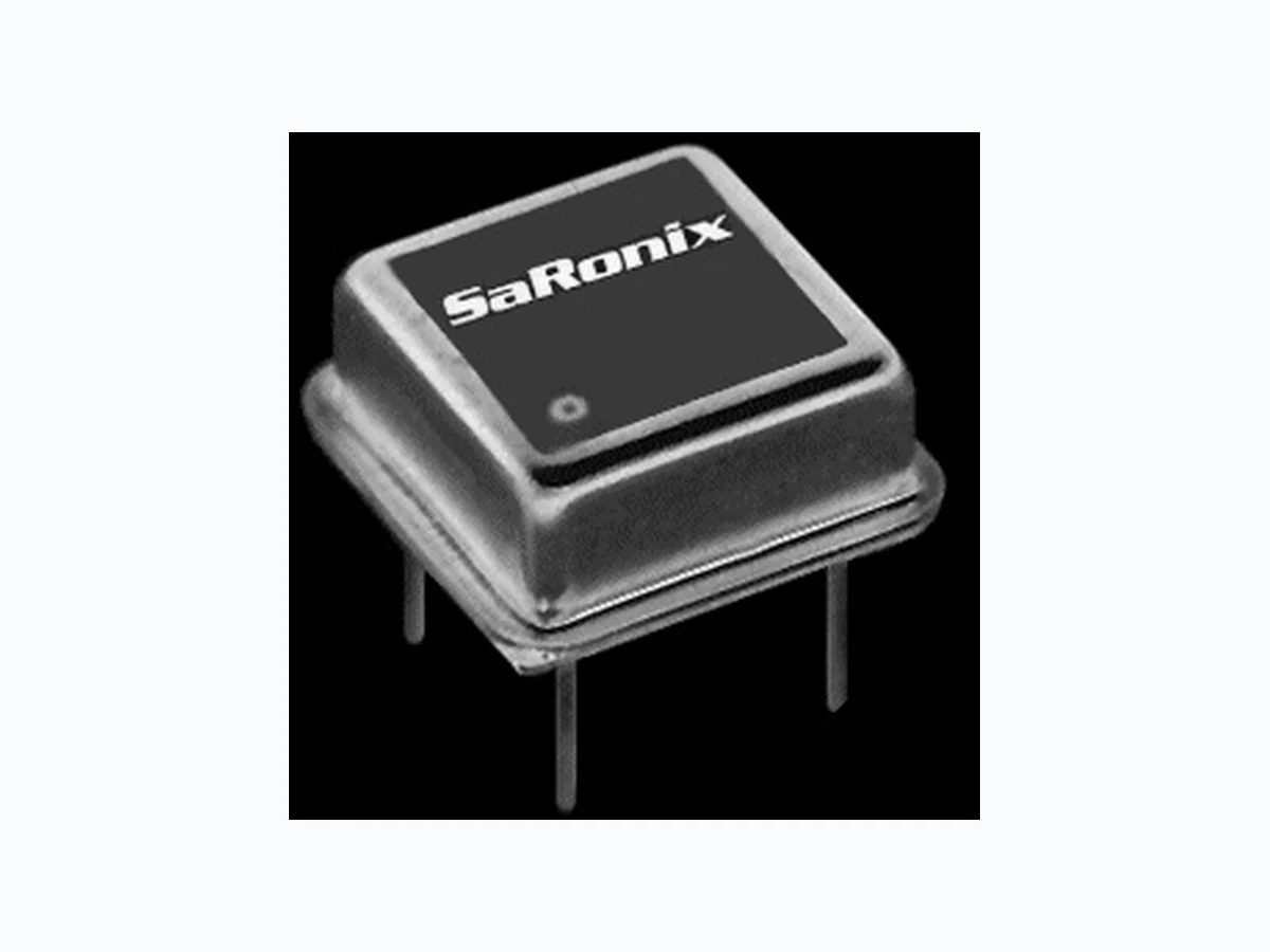
A crystal controlled, low-current oscilla- tor providing precise rise and fall times to drive ACMOS/LVCMOS loads. The tri-state function enables the output to go high impedance. Available in either a 14 or an 8 pin DIP compatible, resistance welded, all metal case. Pin 7 ( or Pin 4 ) is grounded to case to reduce EMI. True SMD DIL 14 version also available, uti- lizing new adaptor technology (see sepa- rate data sheet for package dimensions).
32 MHz to 125 MHz
Frequency Stability: ±20, ±25, ±50 or ±100 ppm over all conditions: calibration tolerance, operating temperature, input voltage change, load change, aging*, shock and vibration. Temperature Range: Operating: Storage: 0 to +70°C or -40 to +85°C -55 to +125°C Supply Voltage: Recommended Operating: Supply Current: 50mA typ, 65mA, 35mA max @ 3.3V Output Drive: Symmetry: 0 to +70°C: -40 to +85°C: ACMOS 32 to 60 MHz 45/55% 45/55% ACMOS 60+ to 125 MHz 45/55% 40/60% (45/55% @ 3.3V) TTL 32 to 60 MHz 45/55% 45/55% TTL 60+ to 125 MHz 45/55% 40/60% *1 year @ +40°C average ambient operating temperature Applications & Features Fiber Channel Gigabit Ethernet HCMOS/ACMOS/LVCMOS MPU's 3.3 or 5V operation High Drive capability Tri-State output standard Short circuit protected output Plastic SMD available, see ST41xH Series data sheet. Ceramic SMD available, see S19xx Series data sheet. True SMD version available, select option S in part number builder (see separate data sheet for package dimen- sions). 2ns max 20% to 80% VDD 1.5ns max 0.5 to 2.5V 10% VDD max or 20% VDD max @ 3.3V 80% VDD min or 80% VDD min @ 3.3V 50Ω ACMOS or 95Ω ACMOS @ 3.3V 13ps max 32 to 72 MHz 20ps max 72+ to 125 MHz, 0 to +70°C 25ps max 72+ to 125 MHz, -40 to +85°C Rise & Fall Times: Logic 0: Logic 1: Load: Period Jitter RMS: Mechanical: MIL-STD-883, Method 2002, Condition B MIL-STD-883, Method 2003 MIL-STD-883, Method 2004, Condition B2 MIL-STD-883, Method 2007, Condition A MIL-STD-202, Method 215 MIL-STD-202, Method 210, Condition A, B or C ( I or J for Gull Wing or SMD) Shock: Solderability: Terminal Strength: Vibration: Solvent Resistance: Resistance to Soldering Heat: Environmental: Gross Leak Test: Fine Leak Test: Thermal Shock: Moisture Resistance: MIL-STD-883, Method 1014, Condition C MIL-STD-883, Method 1014, Condition A2 MIL-STD-883, Method 1011, Condition A MIL-STD-883, Method 1004 Part Numbering Guide ST41 3 0 A – 106.2500 (T) Series Type 3 = 3.3V LVCMOS 5 = 5V TTL 6 = 5V ACMOS Stability Tolerance AA = ±20 ppm, 0 to +70°C A = ±25 ppm, 0 to +70°C B = ±50 ppm, 0 to +70°C C = ±100 ppm, 0 to +70°C E = ±50 ppm, -40 to +85°C F = ±100 ppm, -40 to +85°C Frequency Packing Method (T) = Tape & Reel for SMD versions full reel increments only (200pcs) Blank = Bulk
All specifications are subject to change without notice. SaRonix Crystal Clock Oscillator Technical Data ST41xx Series SaRonix 3.3 & 5V, ACMOS, LVCMOS DS-183 REV C 5.08 .200 (4) Glass Insulators Pin 1 Tri-State Control FULL SIZE PACKAGE 21.0 .825 max max Pin 7 GND 13.0 .510 max SARONIX XTAL OSC 0.91 .036 max .46±.076 .018±.003 15.24±.13 .600±.005 7.75 .305 Pin 14 VDC Pin 8 Output Denotes Pin 1 Tri-State Logic Table Test Circuits Output Waveform Pin 1 Input Logic 1 or NC Logic 0 or GND Pin 8 (5) Output Oscillation High Impedance Required Input Levels on Pin 1: Logic 1 = 2.2V min Logic 0 = 0.8V max HALF SIZE PACKAGE Standard Marking Format Includes Date Code, Frequency, Part Number 13.0 .510 max 0.91 .036 max Denotes Pin 1 5.08 .200 max .46±.08 .018±.003 7.62±.20 .300±.008 120° 120° 120° 1.5 .059 Pin 4 GND Pin 1 Tri-State 13.0 .510 max Pin 5 Output Pin 8 VDD 7.62±.20 .300±.008 Glass Insulators SARONIX Standard Marking Format Includes Date Code, Frequency, Part Number Scale: None (Dimensions in ) mm inches ** Exact location of items may vary 6.35±.51 .250±.020 6.35±.51 .250±.020
2.5 VDC
1.5 VDC
0.5 VDC
20% VDD 50% VDD 80% VDD LOGIC 1 max mA M POWER SUPPLY V M VCC OSCILLATOR Pad 3 Pad 2 .01 µF OUT GND 0.01 µF 50Ω TRI-STATE INPUT (current limited on fixture) ACMOS 50Ω Load mA M POWER SUPPLY V M ACMOS 95Ω Load 0.01 µF 95Ω TEST POINT VCC OSCILLATOR Pad 3 Pad 2 OUT GND .01 µF TRI-STATE INPUT (current limited on fixture) Pad 4 Pad 1 Pad 4 Pad 1 50ΩΩΩΩΩ ACMOS TEST CIRCUIT 95ΩΩΩΩΩ ACMOS TEST CIRCUIT TEST POINT
True SMD Adaptor - 7.57mm High Technical Data SaRonix REV A SaRonix 141 Jefferson Drive • Menlo Park, CA 94025 • USA • 650-470-7700 • 800-227-8974 • Fax 650-462-9894