
DATASHEET SEARCH SITE
Document overview
- Manufacturer or author: Provided By www.digicamel.com(FREE DATASHEET DOWNLOAD SITE)
- PDF pages: 7
Technical content
CMOS Omnipolar High Sensitivity Micropower Hall Switch Packages Features and Benefits 1. Operation down to 2.5V 2. Wide operating voltage range 3. High sensitivity for direct reed switch replacement
applications
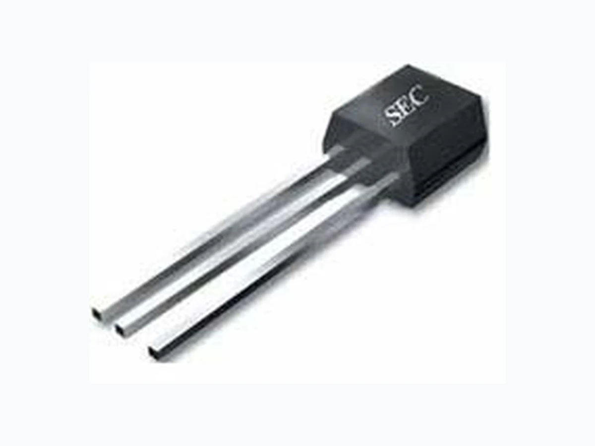
- Omnipolar, output switches with absolute 5. value of North or South pole from magnet 6. Temperature compensation 7. Open-Collector pre-driver 8. 60V maximum withstand voltage 9. Reverse polarity protection 3 pin SIP (suffix UA) 10. Package: TO-92S(SIP) Functional Block Diagram Application Examples 1. Brush-less DC Motor 2. Brush-less DC Fan 3. Revolution counting 4. Speed measurement General Description: The SS40A Omnipolar Hall effect sensor IC is fabricated from mixed signal CMOS technology. It incorporates advanced chopper-stabilization techniques to provide accurate and stable magnetic switch points. The circuit design provides an internally controlled cl ocking mechanism to cycle power to the Hall element and analog signal processing circuits. This serves to place the high current-consuming portions of the circuit into a “Sleep” mode. Periodically the device is “Awakened” by this internal logic and the magnetic flux from the Hall element is evaluated against the predefined thresholds. If the flux density is above or below the B OP/BRP thresholds then the output transistor is driven to change states accordingly. While in th e “Sleep” cycle the output transistor is latched in its previous state. The design has been optimized for service in applications requiring extended operating lifetime in battery powered systems. An internal bandgap regulator is used to provide temperature compensated supply voltage for internal circuits and allows a wide operating supply range. The output transistor of the SS40A will be latched on (B OP) in the presence of a sufficiently strong South or North magnetic field facing the marked side of the package. The output will be latched off (B RP) in the absence of a magnetic field. 1 V1.10 May 1, 2011
CMOS Omnipolar High Sensitivity Micropower Hall Switch Typical Application Circuit SEC's pole-independent sensing technique allows for operation with either a north pole or south pole magnet orientation, enhancing the manufacturability of the device. The state-of-the-art technology provides the same output polarity for either pole face. It is strongly recommended that an external bypass be connected (in close proximity to the Hall sensor) between the supply and ground of the device to reduce both external noise and noise generated by the chopper-stabilization technique. This is especially true due to the relatively high impedance of battery supplies. Functional Block Diagrams VDD Voltage Output Amp Hall Plat e GND 2 V1.10 May 1, 2011
CMOS Omnipolar High Sensitivity Micropower Hall Switch Pin Definitions and Descriptions SIP Pin № Name Type Function
1 VDD Supply Supply Voltage pin
3 OUT Output Open Drain Output pin
2 GND Ground Ground pin
Table 1: Pin definitions and descriptions Absolute Maximum Ratings Parameter Symbol Value Units Supply Voltage (operating) VDD 24 V Reverse Voltage, -V DD -24 V Output Voltage VOUT 30 V Output Current IOUT 50 mA Operating Temperature Range TA -20 to 85 °C Storage Temperature Range TS -55 to 150 °C ESD Sensitivity - 4000 V Table 2: Absolute maximum ratings Exceeding the absolute maximum ratings may cause permanent damage. Exposure to absolute-maximum-rated conditions for extended periods may affect device reliability. DC Operating Parameters: TA = 25℃, VDD= 2.75V. Parameter Symbol Test Conditions Min Typ Max Units Operating Voltage VDD Operating 4.5 5 24 V Supply Current IDD Average 5 10 mA Saturation Voltage VSAT I OUT = 20mA, B>BOP 0.4 0.5 V Output Leakage IOFF B<BRP, VOUT = 20V 0.01 5 µA Output Rise Time tr RL = 1.1K O, CL = 20pf 0.3 1.5 µS Output Fall Time tf RL = 1.1K O, CL = 20pf 0.3 1.5 µS 3 V1.10 May 1, 2011
CMOS Omnipolar High Sensitivity Micropower Hall Switch Table 3: DC electrical characteristics Magnetic Characteristics Operating Parameters: TA = 25°C, VDD = 2.75VDC SS40A Parameter Symbol Min Type Max Units Operating Point BOP - 70 Gs Release Point BRP -70 - Gs Hysteresis B HYST 60 100 Gs Table 4: Magnetic Specifications Output Voltage (V) OFF BOPN BRPS BOPS BRPN ON 3.0 2.0 2.5 0.5 1.0 1.5 -80 -60 -40 -20 0 4020 60 80 Magnetic Flux (Gauss) ESD Protection Human Body Model (HBM) tests according to: Mil. Std. 883F method 3015.7 Limit Values Parameter Symbol Min Max Unit Notes ESD Voltage VESD 4 kV 4 V1.10 May 1, 2011
CMOS Omnipolar High Sensitivity Micropower Hall Switch Performance Characteristics Unique Features CMOS Hall IC Technology The chopper stabilized amplifier uses switched capacitor tech niques to eliminate the amplifier offset voltage, which, in bipolar devices, is a major source of temperature sensit ive drift. CMOS makes this advanced technique possible. The CMOS chip is also much smaller than a bipolar chip, allowing very sophisticated circuitry to be placed in less space. The small chip size also contributes to lower physical stress and less power consumption. Installation Comments Consider temperature coefficients of Hall IC and magneti c, as well as air gap and life time variations. Observe temperature limits during wave soldering. Typical IR solder-reflow profile: – No Rapid Heating and Cooling. – Recommended Preheating for max. 2minutes at 150°C – Recommended Reflowing for max. 5seconds at 240°C 5 V1.10 May 1, 2011
CMOS Omnipolar High Sensitivity Micropower Hall Switch ESD Precautions Electronic semiconductor products are sensitive to Electro Static Discharge (ESD). Always observe Electro Static Discharge control procedures whenever handling semiconductor products. 6 V1.10 May 1, 2011
CMOS Omnipolar High Sensitivity Micropower Hall Switch Package UA, 3-Pin SIP: 7 V1.10 May 1, 2011
Ordering Information
Part No. Pb-free Temperature Code Package Code Packing SS40AEUA YES -40°C to 85°C TO-92 Bulk, 1000 pieces/bag SS40AKUA YES -40°C to 125°C TO-92 Bulk, 1000 pieces/bag SS40ALUA YES -40°C to 150°C TO-92 Bulk, 1000 pieces/bag 4.1 0.1 1 2 1.27 1.9 0.89 451 1.58 0.1 0.76 0.05 313.18 0.1 3 ‐ 0.44 3 ‐ 0.44 0.05 0.05 2.3. 0.1 0.84(Nom) 14 0.5 Notes: 1). Controlling dimension : mm ; 2). Lesds must be free of flash and plating voids ; 3). Do not bend leads within 1 mm of lead to package interface ; Active Area Depth: Sensor Location 1 2 3 40A 06C