

 Download PDF
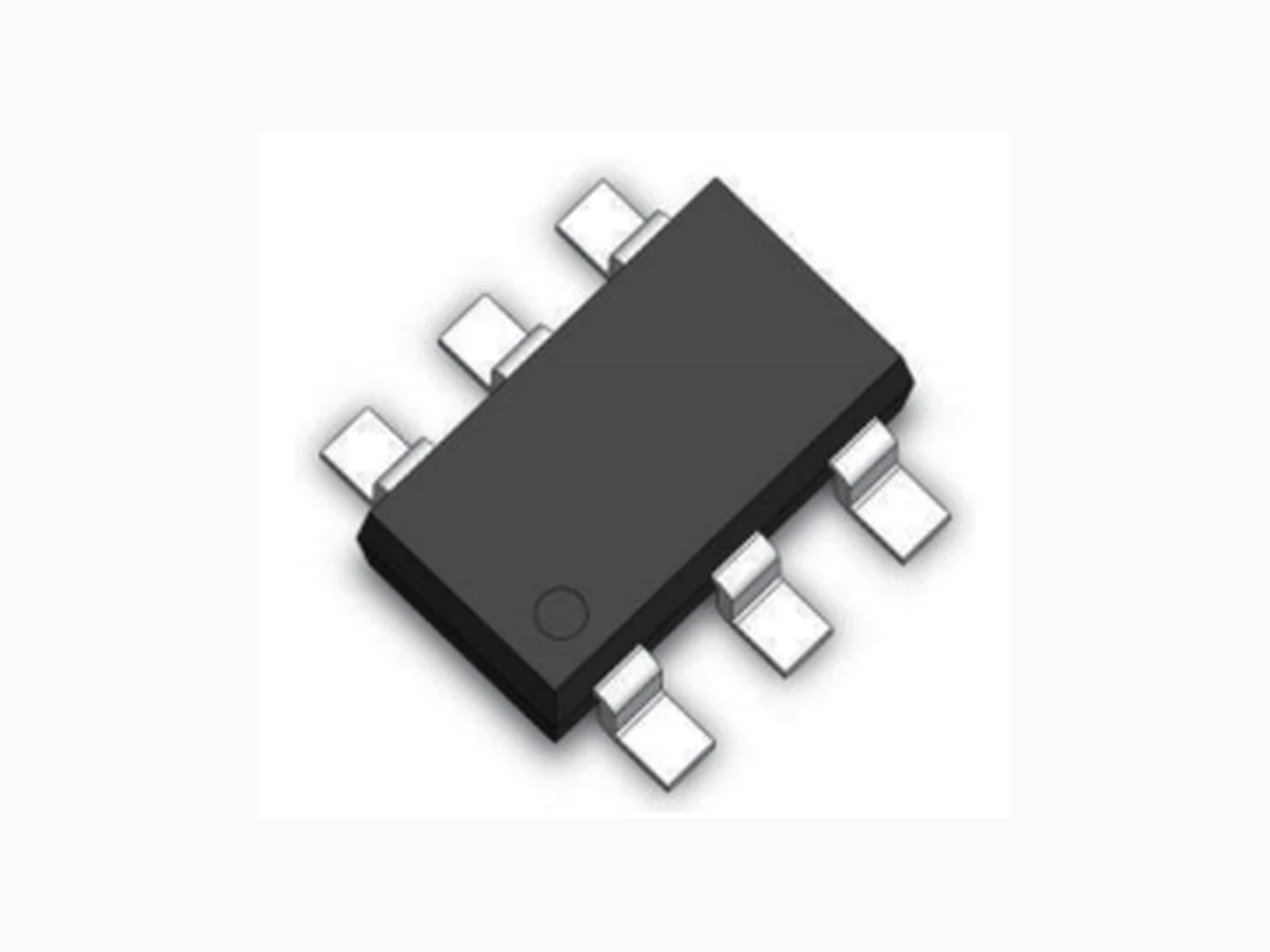
SRV05-4S UNSEMI
Document overview
- PDF pages: 9
Technical content
Page 1
ROHS
Transient Voltage Suppressors for ESD Protection
Description
The SRV05-4S is designed to protect voltage sensitive components from ESD and transient voltage events. This product has been qualified in accordance with the Automotive Electronics Council (AEC) standard Q101 , It is suitable for use in automotive applications. Excellent clamping capability, low leakage, and fast response time, make these parts ideal for ESD protection on designs where board space is at a premium
Feature
Moisture Sensitivity Level (MSL -1) AEC-Q101 qualified 100 Watts Peak Pulse Power per Line (tp=8/20µs) Protects four I/O lines Low clamping voltage
A
Working voltage : 5V Low leakage current IEC61000-4-2 (ESD) ±15kV (air), ±8kV (contact) IEC61000-4-4 (EFT) 40A (5/50ηs) IEC61000-4-5 (Lightning) 5A (8/20μs)
Applications
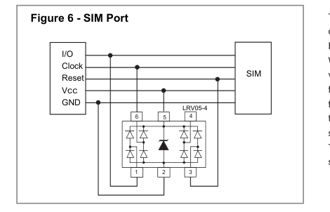
USB 2.0 Power and Data Line Protection Video Graphics Cards Monitors and Flat Panel Displays Digit Video Interface (DVI) 10/100/1000 Ethernet Notebook Computers SIM Ports ATM Interfaces
Mechanical Characteristics

Functional Diagram
Mechanical Data
JEDEC SOT-26 Package Molding Compound Flammability Rating : UL 94V-O Weight 16.0 Milligrams (Approximate) Lead Finish : Lead Free
| Parameter | Symbol | Value | Units |
|---|---|---|---|
| Peak Pulse Power (Tp=8/20μs waveform) | Ppp | 100 | Watts |
| Lead Soldering Temperature | TL | 260 (10 sec.) | °C |
| Storage Temperature Range | TSTG | -55 to +150 | °C |
| Operating Junction Temperature Range | TJ | -40 to +125 | °C |
1/8
Page 2
SRV05-04A
Transient Voltage Suppressors for ESD Protection
ROHS
ROHS
Electrical Characteristics @ 25℃ Unless Otherwise Specified )
| Characteristics | Symbol | Test Conditions | Min. | Typ. | Max. | Unit |
|---|---|---|---|---|---|---|
| Reverse Working Voltage | VRWM | -- | -- | -- | 5.0 | V |
| Reverse Breakdown Voltage | VBR | IT=1mA; | 6.0 | -- | -- | V |
| Reverse Leakage Current | IR | VRWM =5.0V, T=25°C; | -- | -- | 1.0 | μA |
| Positive Clamping Voltage | VC | Ipp=1A, Tp =8/20μs; | -- | -- | 12.5 | V |
| Ipp =4A, Tp =8/20us; | -- | -- | 17.5 | V | ||
| Junction capacitance | CJ | VR= 0V,f= 1MHz; | -- | 1.2 | -- | pF |
Characteristic Curves
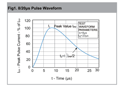
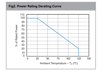
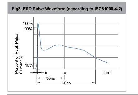
2/8
Page 3
Transient Voltage Suppressors for ESD Protection
ROHS
SOT-26 Package Outline & Dimensions
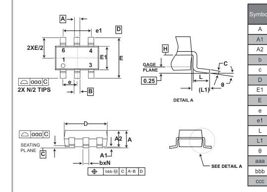
| Symbol | Inches | Millimeters | ||||
|---|---|---|---|---|---|---|
| Min. | Nom. | Max. | Min. | Nom. | Max. | |
| A | 0.035 | -- | 0.057 | 0.90 | -- | 1.45 |
| A1 | 0.000 | -- | 0.006 | 0.00 | -- | 0.15 |
| A2 | 0.035 | 0.045 | 0.051 | 0.90 | 1.15 | 1.30 |
| b | 0.010 | -- | 0.020 | 0.25 | -- | 0.50 |
| c | 0.003 | -- | 0.009 | 0.08 | -- | 0.22 |
| D | 0.110 | 0.114 | 0.122 | 2.80 | 2.90 | 3.10 |
| E1 | 0.060 | 0.063 | 0.069 | 1.50 | 1.60 | 1.75 |
| E | 0.110BSC | 2.80BSC | ||||
| e | 0.037BSC | 0.95BSC | ||||
| e1 | 0.075BSC | 1.90BSC | ||||
| L | 0.012 | 0.018 | 0.024 | 0.30 | 0.45 | 0.60 |
| L1 | (0.024) | (0.60) | ||||
| θ | 0⁰ | -- | 10⁰ | 0⁰ | -- | 10⁰ |
| aaa | 0.004 | 0.10 | ||||
| bbb | 0.008 | 0.20 | ||||
| ccc | 0.008 | 0.20 | ||||

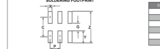
| Symbol | Inches | Millimeters |
|---|---|---|
| C | (0.098) | (2.50) |
| G | 0.055 | 1.40 |
| P | 0.037 | 0.95 |
| X | 0.024 | 0.60 |
| Y | 0.043 | 1.10 |
| Z | 0.141 | 3.60 |

Ordering Information
| Device | Marking | Package | Quantity | Reel Size |
| SRV05-4S | V05 | SOT-26 | 3,000pcs/Reel | 7 inch |
3/8
Page 4
Transient Voltage Suppressors for ESD Protection
ROHS
Applications information
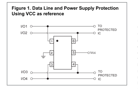
Device Connection Options for Protection of Four High-Speed Data Lines
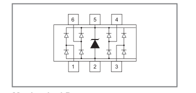
The LRV05-4 is designed to protect four data lines from transient over-voltages by clamping them to a fixed reference. When the voltage on the protected line exceeds the reference voltage (plus diode VF) the steering diodes are forward biased, conducting the transient current away from the sensitive circuitry. Data lines are connected at pins 1, 3, 4 and 6. The negative reference (REF1) is connected at pin 2. This pin should be connected directly to a ground plane on the board for best results. The path length is kept as short as possible to minimize parasitic inductance. The positive
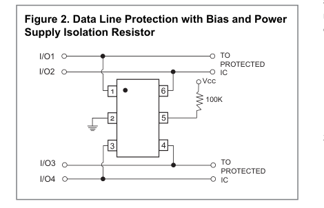
reference (REF2) is connected at pin 5. The options for connecting the positive reference are as follows:
- To protect data lines and the power line, connect pin 5 directly to the positive supply rail (VCC). In this configuration the data lines are referenced to the supply voltage. The internal TVS diode prevents over-voltage on the supply rail (See Figure1).
- The LRV05-4 can be isolated from the power supply by adding a series resistor between pin 5 and VCC. A value of 100kΩ is recommended. The internal TVS and steering diodes remain biased, providing the advantage of lower capacitance (See Figure2).
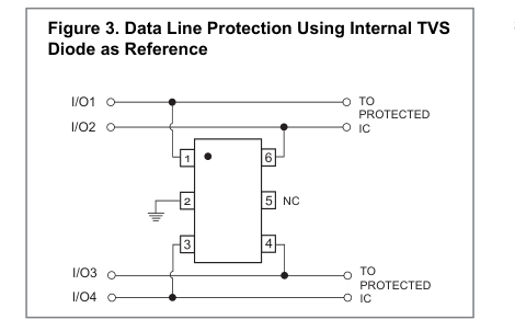
- In applications where no positive supply reference is available, or complete supply isolation is desired, the internal TVS may be used as the reference. In this case, pin 5 is not connected. The steering diodes will begin to conduct when the voltage on the protected line exceeds the working voltage of the TVS (plus one diode drop) (See Figure3).
4/8
Page 5
Transient Voltage Suppressors for ESD Protection
ROHS
Applications information (Continue)
Video Interface Protection
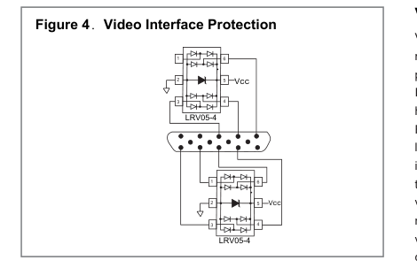
Video interfaces are susceptible to transient voltages resulting from electrostatic discharge (ESD) and “hot plugging” cables. If left unprotected, the video interface IC may be damaged or even destroyed. Protecting a high-speed video port presents some unique challenges. First, any added protection device must have extremely low capacitance and low leakage current so that the integrity of the video signal is not compromised. Second, the protection component must be able to absorb high voltage transients without damage or degradation. As a minimum, the device should be rated to handle ESD voltages per IEC61000-4-2, level 4 (±15kV air, ±8kV contact). The clamping voltage of the device (when
conducting high current ESD pulses) must be sufficiently low enough to protect the sensitive CMOS IC. If the clamping voltage is too high, the “protected” device may latch-up or be destroyed. Finally, the device must take up a relatively small amount of board space, particularly in portable applications such as notebooks and handhelds. The LRV05-4 is designed to meet or exceed all of the above criteria. A typical video interface protection circuit is shown in Figure 4. All exposed lines are protected including R, G, B, H-Sync, V-Sync, and the ID lines for plug and play monitors.
Universal Serial Bus ESD Protection
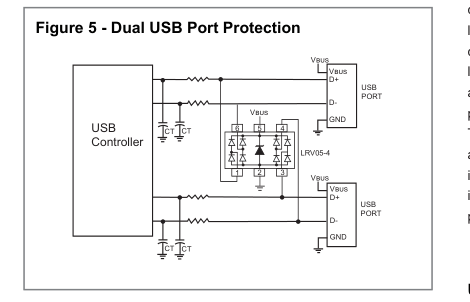
The LRV05-4 may also be used to protect the USB ports on monitors, computers, peripherals or portable systems. Each device will protect up to two USB ports (Figure5). When the voltage on the data lines exceed the bus voltage (plus one diode drop), the internal rectifiers are forward biased conducting the transient current away from the protected controller chip. The TVS diode directs the surge to ground. The TVS diode also acts to suppress ESD strikes directly on the voltage bus. Thus, both power and data pins are protected with a single device.
5/8
Page 6
Applications information (Continue)
DVI Protection
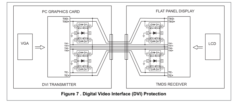
The small geometry of a typical digital-visual interface (DVI) graphic chip will make it more susceptible to electrostatic discharges (ESD) and cable discharge events (CDE). Transient protection of a DVI port can be challenging. Digital-visual interfaces can often transmit and receive at a rate equal to or above 1Gbps. The high-speed data transmission requires the protection device to have low capacitance to maintain signal integrity and low clamping voltage to reduce stress on the protected IC. The LRV05-4 has a low typical insertion loss of <0.4dB at 1GHz (I/O to ground) to ensure signal integrity and can protect the DVI interface to the 8kV contact and 15kV air ESD per IEC
61000-4-2 and CDE.
Transient Voltage Suppressors for ESD Protection
ROHS
Figure 7 shows how to design the LRV05-4 into the DVI circuit on a flat panel display and a PC graphic card. The LRV05-4 is configured to provide common mode and differential mode protection. The internal TVS of the LRV05-4 acts as a 5 volt reference. The power pin of the DVI circuit does not come out through the connector and is not subjected to external ESD pulse; therefore, pin 5 should be left unconnected. Connecting pin 5 to Vcc of the DVI circuit may result in damage to the chip from ESD current.
10/100 ETHERNET PROTECTION
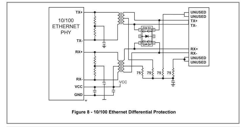
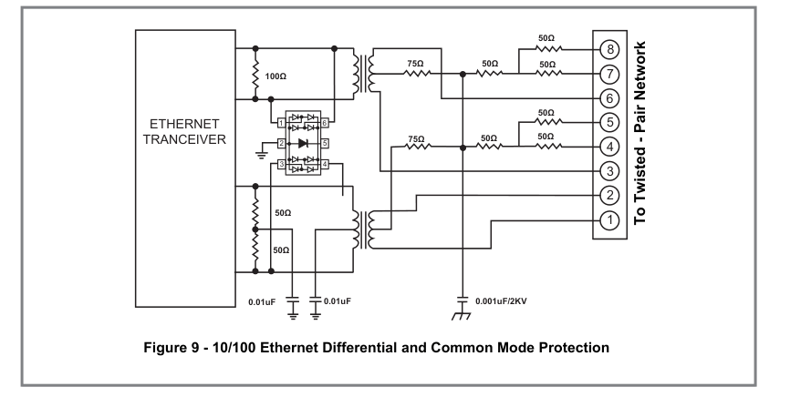
Ethernet ICs are vulnerable to damage from electro-static discharge (ESD). The internal protection in the PHY chip, if any, often is not enough due to the high energy of the discharges specified by IEC 61000-4-2. If the discharge is catastrophic, it will destroy theprotected IC. If it is less severe, it will cause latent failures that are very difficult to find. 10/100 Ethernet operates at 125MHz clock over a twisted pair interface. In a typical system, the twisted-pair interface for each port consists of two differential signal pairs: one for the transmitter and one for the receiver, with the transmitter input
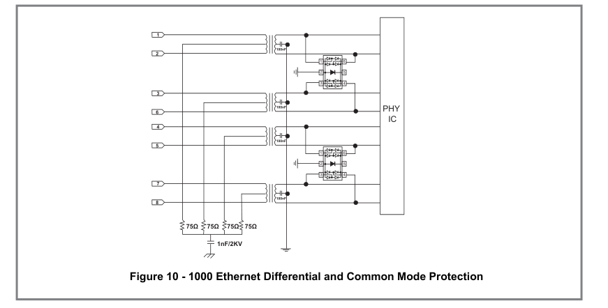
6/8 being the most sensitive to damage. The fatal discharge occurs differentially across the transmit or receive line pair and is capacitively coupled through the transformer to the Ethernet chip. Figure 8 shows how to design the LRV05-4 on the line side of a 10/100 ethernet port to provide differential mode protection. The common mode isolation of the transformer will provide common mode protection to the rating of the transformer isolation which is usually >1.5kV. If more common mode protection is needed, figure 9 shows how to design the LRV05-4 on the IC side of the 10/100.
Page 7
Transient Voltage Suppressors for ESD Protection
ROHS
Applications information (Continue)
7/8
Page 8
Transient Voltage Suppressors for ESD Protection
ROHS
Applications information (Continue)
8/8
Page 9
ROHS
ROHS
Disclaimer
UNSEMI RESERVES THE RIGHT TO MAKE CHANGE ON OUR PRODUTS , PRODUCTS SPECIFICATION
AND DATA WITHOUT NOTICE TO IMPROVE RELIABILITY, FUNCTION OR DESIGN OR OTHERWISE.
UN SEMICONDUCTOR LIMITED its affiliates, agents, and employees, and all persons acting on its or their
behalf (collectively, “UNSEMI”)does not give any representations or warranties for any errors, inaccuracies or
incompleteness contained in any datasheet or in any other disclosure relating to any product.
In no event shall UNSEMI be liable for any indirect, incidental, punitive, special or consequential damages
(including any and all implied warranties, warranties of fitness for particular purpose, non-infringement and
merchantability.) whether or not such damages are based on tort (including negligence), warranty, breach of
contract or any other legal theory.
Statements regarding the suitability of products for certain types of applications are based on UNSEMI
knowledge of typical requirements that are often placed on UNSEMI products in generic applications. Such
statements are not binding, statements about the suitability of products for a particular application. It is the
customer's responsibility to validate that a particular product with the properties described in the product
specification is suitable for use in a particular application. Parameters provided in datasheets or specifications
may vary in different applications and performance may vary over time. All operating parameters, including typical
parameters, must be validated for each customer application by the customer's technical experts. Product
specifications do not expand or otherwise modify UNSEMI's terms and conditions of purchase, including but not
limited to the warranty expressed therein.
Unless otherwise agreed in writing, UNSEMI product is not designed, authorized or warranted to be suitable for
use in medical life-saving, or life-sustaining application , nor in applications where failure or malfunction of a
UNSEMI product can reasonably be expected to result in personal injury, death or severe property or environmental
damage. UNSEMI and its suppliers accept no liability for inclusion or use of UNSEMI products in such equipment or
applications and therefore such inclusion and/or use is at the customer's own risk.
All referenced brands, product names, service names and trademarks are the property of their respective owners.