
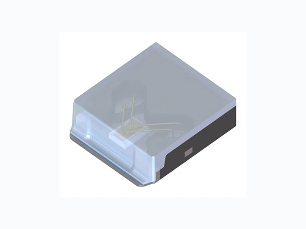
SPLS1L90A_3A01 OSRAM
Document overview
- Manufacturer or author: Provided By www.digicamel.com(FREE DATASHEET DOWNLOAD SITE)
- PDF pages: 20
Technical content
SPL S1L90A_3 A01 1 Version 1.0 | 2020-11-18 Produktdatenblatt | Version 1.1 www.osram-os.com
Applications
SPL S1L90A_3 A01 SMT Laser
1 Channel SMT Laser in QFN package
—3D Sensing —CCTV Surveillance —Industrial Automation (Machine Controls, Light Barriers, Vision Controls) —LIDAR, Pre-Crash, ACC —Measurement Levelling Features: —Qualifications: The product qualification test plan is based on the guidelines of AEC-Q102, failure mechanism based Stress Test Qualification for Discrete Optoelectronic Semiconductors in Automotive applications. —Laser wavelength 905 nm —1 channel pulsed laser module —Suited for short laser pulses from 1 to 100 ns —SMT device
Ordering Information
Type Peak output power Ordering Code typ. Popt SPL S1L90A_3 A01 120 W Q65112A6166
SPL S1L90A_3 A01 2 Version 1.0 | 2020-11-18 Maximum Ratings TS = 25 °C Parameter Symbol Values Operating temperature Top min. max. -40 °C 105 °C Storage temperature Tstg min. max. -40 °C 125 °C Junction temperature Tj max. 125 °C Output power Popt max. 0.24 W Forward current dc = 0.2 % IF max. 40 A Pulse width (FWHM) tP max. 100 ns Duty cycle dc max. 0.2 % Reverse voltage 1) VR max. 45 V
SPL S1L90A_3 A01 3 Version 1.0 | 2020-11-18 Characteristics IF = 40 A; tp = 100 ns; D = 0.01 %; TS = 25 °C Parameter Symbol Values Number of channels N typ. 1 Operating voltage Vop typ. 11 V Peak wavelength λpeak typ. 908 nm Centroid wavelength 2) λcentroid min. typ. max. 895 nm 905 nm 915 nm Spectral bandwidth (FWHM) ∆λ min. typ. max. 3 nm 7 nm 12 nm Peak output power 3) Popt min. typ. max. 105 W 125 W 145 W Beam divergence (FWHM) parallel to pn-junction Θ‖ min. typ. max. 3 ° 10 ° 13 ° Beam divergence (FWHM) perpendicular to pn-junction Θ┴ min. typ. max. 20 ° 25 ° 30 ° Beam divergence (1/e²) parallel to pn-junction Θ‖ min. typ. max. 10 ° 13 ° 16 ° Beam divergence (1/e²) perpendicular to pn-junction Θ┴ min. typ. max. 35 ° 40 ° 50 ° Threshold current Ith typ. 0.6 A Laser aperture (FWHM) parallel to pn-junction W|| typ. 220 µm Laser aperture (FWHM) perpendicular to pn-junction W┴ typ. 10 µm Thermal resistance junction solder point real 4) RthJS real typ. max.
31 K / W
36 K / W
SPL S1L90A_3 A01 4 Version 1.0 | 2020-11-18 Relative Spectral Emission 5), 6) Ie,rel = f (ʎ); IF = 40A; Popt = 125W; tp = 100ns; D = 0.01% 8800 λ OHF00565 0.25 0.50 0.75 1.00 Ιrel nm890 900 910 930 Far-Field Distribution Perpendicular to pn-Junction 5), 6) Irel = f (Θ⊥); Popt = 125W; tp = 100ns; D = 0.01% OHL00756 0-40 0.25 0.50 0.75 1.00 Deg Irel θ -30 -20 -10 0 10 20 40
SPL S1L90A_3 A01 5 Version 1.0 | 2020-11-18 Far-Field Distribution Parallel to pn-Junction 5), 6) Irel = f (ΘII); Popt = 125W; tp = 100ns; D = 0.01% Deg-30 θ 0.25 0.50 0.75 Irel 1.00 OHF03755 -20 -10 0 10 30 Near-Field Distribution Parallel to pn-Junction 5), 6) Irel = f (ΘII); Popt = 125W; tp = 100ns; D = 0.01%
SPL S1L90A_3 A01 6 Version 1.0 | 2020-11-18 Near-Field Distribution Perpendicular to pn-Junction 5), 6) Irel = f (Θ⊥); Popt = 125W; tp = 100ns; D = 0.01% Optical Output Power 5), 6) Popt = f (IF)
SPL S1L90A_3 A01 7 Version 1.0 | 2020-11-18 Centroid Wavelength 5) ʎcentroid = f (TJ); IF = 40A; tp = 100ns; D = 0.01% Centroid Wavelength 5) ʎcentroid = f (TJ); IF = 40A; tp = 100ns; D = 0.01% Centroid Wavelength 5) λcentroid = f(TS); IF = 40A; tp = 100ns; D = 0.01% Centroid Wavelength 5) λcentroid = f(TS); IF = 40A; tp = 100ns; D = 0.01%
SPL S1L90A_3 A01 8 Version 1.0 | 2020-11-18 Peak Output Power Popt = f (TJ); IF = 40A; tp = 100ns; D = 0.01% Peak Output Power Popt = f(TS); IF = 40A; tp = 100ns; D = 0.01% Permissible Pulse Handling Capability IF = f (tp); D = parameter; Popt, typ; Rthjs, typ; TS = 85°C (typ) Permissible Pulse Handling Capability IF = f (tp); D = parameter; Popt, min; Rthjs, max; TS = 85°C
SPL S1L90A_3 A01 9 Version 1.0 | 2020-11-18 Permissible Pulse Handling Capability IF = f (tp); D = parameter; Popt, typ; Rthjs, typ; TS = 105°C Permissible Pulse Handling Capability IF = f (tp); D = parameter; Popt, min; Rthjs, max; TS = 105°C
SPL S1L90A_3 A01 10 Version 1.0 | 2020-11-18 Dimensional Drawing 7) Further Information: Approximate Weight: 8.0 mg
SPL S1L90A_3 A01 11 Version 1.0 | 2020-11-18 Recommended Solder Pad 7)
SPL S1L90A_3 A01 12 Version 1.0 | 2020-11-18 Reflow Soldering Profile Product complies to MSL Level 3 acc. to JEDEC J-STD-020E 00 s OHA04525 100 150 200 250 300 50 100 150 200 250 300 t T St t Pt Tp240 ˚C 217 ˚C 245 ˚C 25 ˚C L Profile Feature Symbol Pb-Free (SnAgCu) Assembly Unit Minimum Recommendation Maximum Ramp-up rate to preheat*) 25 °C to 150 °C 2 3 K/s Time tS TSmin to TSmax tS 60 100 120 s Ramp-up rate to peak*) TSmax to TP 2 3 K/s Liquidus temperature TL 217 °C Time above liquidus temperature tL 80 100 s Peak temperature TP 245 260 °C Time within 5 °C of the specified peak temperature TP - 5 K tP 10 20 30 s Ramp-down rate* TP to 100 °C 3 6 K/s Time 25 °C to TP 480 s All temperatures refer to the center of the package, measured on the top of the component * slope calculation DT/Dt: Dt max. 5 s; fulfillment for the whole T-range
SPL S1L90A_3 A01 13 Version 1.0 | 2020-11-18 Taping 7)
SPL S1L90A_3 A01 14 Version 1.0 | 2020-11-18 Tape and Reel 8) Reel Dimensions A W Nmin W1 W2 max Pieces per PU 180 mm 12 + 0.3 / - 0.1 mm 60 mm 12.4 + 2 mm 18.4 mm 500
SPL S1L90A_3 A01 15 Version 1.0 | 2020-11-18 Barcode-Product-Label (BPL) Dry Packing Process and Materials 7) OHA00539 OSRAM Moisture-sensitive label or print Barcode label Desiccant Humidity indicator Barcode label OSRAM Please check the HIC immidiately after bag opening. Discard if circles overrun. Avoid metal contact. WET Do not eat. Comparator check dot parts still adequately dry. examine units, if necessary examine units, if necessary 15% 10%bake units bake units If wet, change desiccant If wet, Humidity Indicator MIL-I-8835 If wet, M oisture Level 3 Floor tim e 168 Hours M oisture Level 6 Floor tim e 6 Hours a) Hum idity Indicator Card is > 10% when read at 23 ˚C ± 5 ˚C, or reflow, vapor-phase reflow, or equivalent processing (peak package 2. After this bag is opened, devices that will be subjected to infrared 1. Shelf life in sealed bag: 24 m onths at < 40 ˚C and < 90% relative hum idity (RH). M oisture Level 5a at factory conditions of (if blank, seal date is identical with date code). a) M ounted within b) Stored at body tem 3. Devices require baking, before m ounting, if: Bag seal date M oisture Level 1 M oisture Level 2 M oisture Level 2a4. If baking is required, b) 2a or 2b is not m et. Date and tim e opened: reference IPC/JEDEC J-STD-033 for bake procedure. Floor tim e see below If blank, see bar code label Floor tim e > 1 Year Floor tim e 1 Year Floor tim e 4 W eeks10% RH. M oisture Level 4 M oisture Level 5 ˚C). OPTO SEMICONDUCTORS MOISTURE SENSITIVE This bag contains CAUTION Floor tim e 72 Hours Floor tim e 48 Hours Floor tim e 24 Hours 30 ˚C/60% RH. LEVEL If blank, see bar code label Moisture-sensitive product is packed in a dry bag containing desiccant and a humidity card according JEDEC-STD-033.
SPL S1L90A_3 A01 16 Version 1.0 | 2020-11-18 Notes Depending on the mode of operation, these devices emit highly concentrated visible and non visible light which can be hazardous to the human eye. Products which incorporate these devices have to follow the safety precautions given in IEC 60825-1. Subcomponents of this device contain, in addition to other substances, metal filled materials including silver. Metal filled materials can be affected by environments that contain traces of aggressive substances. There- fore, we recommend that customers minimize device exposure to aggressive substances during storage, production, and use. Devices that showed visible discoloration when tested using the described tests above did show no performance deviations within failure limits during the stated test duration. Respective failure limits are described in the IEC60810. Tape and Reel: Packing unit can vary 2 % from the stated value. For further application related information please visit www.osram-os.com/appnotes
SPL S1L90A_3 A01 17 Version 1.0 | 2020-11-18 Disclaimer Attention please! The information describes the type of component and shall not be considered as assured characteristics. Terms of delivery and rights to change design reserved. Due to technical requirements components may contain dangerous substances. For information on the types in question please contact our Sales Organization. If printed or downloaded, please find the latest version on the OSRAM OS website. Packing Please use the recycling operators known to you. We can also help you – get in touch with your nearest sales office. By agreement we will take packing material back, if it is sorted. You must bear the costs of transport. For packing material that is returned to us unsorted or which we are not obliged to accept, we shall have to invoice you for any costs incurred. Product and functional safety devices/applications or medical devices/applications OSRAM OS components are not developed, constructed or tested for the application as safety relevant component or for the application in medical devices. OSRAM OS products are not qualified at module and system level for such application. In case buyer – or customer supplied by buyer – considers using OSRAM OS components in product safety devices/applications or medical devices/applications, buyer and/or customer has to inform the local sales partner of OSRAM OS immediately and OSRAM OS and buyer and /or customer will analyze and coordi- nate the customer-specific request between OSRAM OS and buyer and/or customer.
SPL S1L90A_3 A01 18 Version 1.0 | 2020-11-18 Glossary 1) Reverse Operation: This product is intended to be operated applying a forward current within the specified range. Applying any continuous reverse bias or forward bias below the voltage range of light emission shall be avoided because it may cause migration which can change the electro-optical char- acteristics or damage the LED. 2) Wavelength: The wavelengths are measured with a tolerance of ±1 nm. 3) Brightness: The brightness values are measured with a tolerance of ±11%. 4) Thermal resistance: junction - soldering point, of the device only, mounted on an ideal heatsink (e.g. metal block) 5) Typical Values: Due to the special conditions of the manufacturing processes of semiconductor devic- es, the typical data or calculated correlations of technical parameters can only reflect statistical figures. These do not necessarily correspond to the actual parameters of each single product, which could dif- fer from the typical data and calculated correlations or the typical characteristic line. If requested, e.g. because of technical improvements, these typ. data will be changed without any further notice. 6) Testing temperature: TA = 25°C (unless otherwise specified) 7) Tolerance of Measure: Unless otherwise noted in drawing, tolerances are specified with ±0.1 and dimensions are specified in mm. 8) Tape and Reel: All dimensions and tolerances are specified acc. IEC 60286-3 and specified in mm.
SPL S1L90A_3 A01 19 Version 1.0 | 2020-11-18
Revision History
1.0 2020-11-17 Features
SPL S1L90A_3 A01 20 Version 1.0 | 2020-11-18 Published by OSRAM Opto Semiconductors GmbH Leibnizstraße 4, D-93055 Regensburg www.osram-os.com © All Rights Reserved.