

 Download PDF
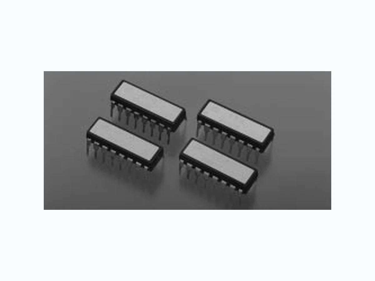
SPG8640AN ETC1
Document overview
- Manufacturer or author: Provided By www.digicamel.com(FREE DATASHEET DOWNLOAD SITE)
- PDF pages: 2
Technical content
Features
- Capable of selecting 57 varieties of frequency output
- Use of CMOS IC enables low current consumption
- Easy-to-mount DIP 16 pin type
- Most types held ex-stock Reset Timing Dimensions (mm) Block Diagram Crystal Oscillators - Programmable - Seiko Epson Item Symbol Min. T yp. Max. Unit Remarks L input voltage V IL 0 0.8 V H input voltage V IH VDD -1.0 V DD L input current (Reset) IRL -30 -5 µA Reset=V SS H input current (Reset) IRH 0.5 µA Reset=V DD L input current I IL -0.5 µA (input terminal except for Reset) H input current I IH 53 0 µ A (input terminal except for Reset) L output voltage V OL 0.4 V I OL =1.6mA H output voltage V OH VDD -1.0 V I OH =40µA L output current I OL 1.6 mA V OL =0.4V H output current I OH -40 µA V OH =VDD -1.0V Output rise time t TLH 30 60 nS Output fall time t THL 25 50 nS Duty 40 60 % Except in the case of 1/3 and 1/5 Min. reset pulse width tRW 1.0 µS Reset delay time t R 1.0 µS Reset release t E tw -1/2 to (*1) tw (*2) synchronous error External signal input FIN 1M Hz 8640N only frequency External signal input tIN 0.5 µS 8640N only plus width Oscillation startup time tOSC 0.2 1 sec. (*3) (*1) to-oscillation source cycle. (*2) tw=1/2 cycle of preset frequency (*3) for more than 1mS until VDD=0.4.5V. Time at 4.5V is to be zero Item Symbol Specifications Remarks Model name 8650 ? Input clock frequency 1MHz MAX Current consumption lop about 2mA No load condition Item Symbol Specifications Remarks Model name 8640AN 8640BN 8640CN 8650A 8650B 8650C 8650D 8650E 8651A 8651B 8651E For output frequency, refer to the Oscillation source frequency fo 600kHz 1MHz 769kHz 60kHz 100kHz 96kHz 153.6kHz 32.768kHz 60kHz 100kHz 32.768kHz table on the next page Power source Max. supply voltage V DD -GND -0/3V ~ +7.0V voltage Operating voltage V DD 5.0V ± 0.5V Temperature Storage temp. T STG -55°C ~ +125°C -30°C ~ +80°C range Operating temp. T OPR -10°C ~ +70°C Soldering condition (lead part) T SOL Under 260°C within 10 sec. Package should be less than 150°C Frequency tolerance ∆f/f ±100ppm ±50ppm ±5ppm (1*) V DD =5V, Ta= 25°C Frequency/temp. characteristics +10/-120ppm V DD =5V, Ta=10 ~ 70°C Frequency Voltage characteristics ±20ppm ±10ppm ±20ppm ±10ppm ±5ppm V DD =4.5 ~ 5.5V Aging fa ±5ppm/year max. ±3ppm/year max V DD =5V, Ta=25°C (*1) Frequency tolerance of 8651 system shows the value guaranteed at the time of shipment
TEL: +44 1635 528520 FAX: +44 1635 528443 16 15 14 13 12 11 10 9 1 2 34 567 8 Crystal Oscillators - Programmable - Seiko Epson SPG Series Baud Rate Generator 8640CN CTL1 CTL2 CTL3 CTL4 CTL5 CTL6 Output frequency Baud rate output example (kH) (fo/16)(bits/sec) 0 0 0 0 0 0 768k 48000 1 0 1 0 0 0 153.6 9600 0 0 1 0 0 0 76.8 4800 0 1 0 0 0 1 38.4 2400 1 0 0 0 0 1 19.2 1200 8650C CTL1 CTL2 CTL3 CTL4 CTL5 CTL6 Output frequency Baud rate output example (kH) (fo/16)(bits/sec) 0 0 0 0 0 0 96.0 6000 1 0 1 0 0 0 19.2 1200 0 0 1 0 0 0 9.6 600 0 1 0 0 0 1 4.8 300 0 1 1 0 0 1 3.2 200 1 0 0 0 0 1 2.4 150 1 1 0 0 0 1 1.6 100 1 1 1 0 0 1 0.8 50 8650D CTL1 CTL2 CTL3 CTL4 CTL5 CTL6 Output frequency Baud rate output example (kH) (fo/16)(bits/sec) 0 0 0 0 0 0 153.6 9600 0 0 0 0 0 1 76.8 4800 0 0 0 0 1 0 38.4 2400 0 0 0 0 1 1 19.2 1200 0 0 0 1 0 1 4.8 300 0 1 1 1 0 0 3.2 200 0 0 0 1 1 0 2.4 150 1 1 0 1 0 0 1.6 100 0 0 0 1 1 1 1.2 75 1 1 1 1 0 0 0.8 50 Explanation of T erminals T erminal Function Name CTL1 to 6 Programs dividing ratio. (pull-down resistor incorporated) OUT Output frequency preset by CTL1~6. (Refer to the setting procedure of output frequency) FOUT Constantly outputs the oscillation source frequency of built-in quartz crystal. RESET Stops output at RESET=“L ”. (Pull up resistor incorporated) TEST Used for the input terminal for testing. When CTL4 is H, output will be 1000 times larger than the preset value at TEST -“H”. (Pull-down resistor incorporated) EXC Serves as input terminal when using an external clock by (8640N only) changing to the built-in oscillator. Effective only when CSEL is H. CSEL When this terminal is made H, the external clock is selected (8640N only) (Pull down resistor incorporated). Note: treatment of empty terminals. When RESET terminal is not used, this should be connected to VDD, when TEST terminal, CSEL terminal, and CTL1 to 6 terminals are not used, to GND. Additional explanation of terminals for 8650D series Clock Clock input (max. 1MHz) ENABLE Be sure to connect to V DD Setting of Divider Output CTL1 CTL2 CTL3 Dividing ratio 0 0 0 1/1 0 0 1 1/10 0 1 0 1/2 0 1 1 1/3 1 0 0 1/4 1 0 1 1/5 1 1 0 1/6 1 1 1 1/12 *0 = L 1 = H CTL4 CTL5 CTL6 Dividing ratio 0 0 0 1/1 (1/ 0 0 1 1/10 (1/ 2) 0 1 0 1/10 2 (1/22) 0 1 1 1/10 3 (1/23) 1 0 0 1/10 4 (1/24) 1 0 1 1/10 5 (1/25) 1 1 0 1/10 6 (1/26) 1 1 1 1/10 7 (1/27) ()8650D CTL6 CTL3 Setting of Output Frequency 8640AN Set terminal CTL4 0 0 0 0 1 1 1 1 CTL5 0 0 1 1 0 0 1 1 CTL1 CTL2 0 1 0 1 0 1 0 1 000 600K 60K 6K 600 60 6 0.6 0.06 001 60K 6K 600 60 6 0.6 0.06 0.006 010 300K 30K 3K 300 30 3 0.3 0.03 011 200K 20K 2K 200 20 2 0.2 0.02 100 150K 15K 1.5K 150 15 1.5 0.15 0.015 101 120K 12K 1.2K 120 12 1.2 0.12 0.012 110 100K 10K 1K 100 10 1 0.1 0.01 111 50K 5K 500 50 5 0.5 0.05 0.005 CTL6 CTL3 CTL6 CTL3 CTL6 CTL3 CTL6 CTL3 Note: Lower digits are omitted Terminal Connection NC: Do not connect to the external terminal. 1. NC 16. V DD 2. CTL 3 15. NC 3. CTL 2 14. RESET 4. CTL 1 13. NC (CSEL) 5. CTL 6 12. NC(EXC) 6. CTL 5 11. F OUT 7. CTL 4 10. TEST 8. GND 9. OUT ( ) Shown 8640N only For 8650 O 11. NC 12. Clock 13. Enable 8640BN Set terminal CTL4 0 0 0 0 1 1 1 1 CTL5 0 0 1 1 0 0 1 1 CTL1 CTL2 0 1 0 1 0 1 0 1 000 1M 100K 10K 1K 100 10 1 1/10 001 100K 10K 1K 100 10 1 1/10 1/100 010 500K 50K 5K 500 50 5 1/2 1/20 100 250K 25K 2.5K 250 25 2.5 1/4 1/40 101 200K 20K 2K 200 20 2 1/5 150 8650A 8651A Set terminal CTL4 0 0 0 0 1 1 1 1 CTL5 0 0 1 1 0 0 1 1 CTL1 CTL2 0 1 0 1 0 1 0 1 000 60K 6K 600 60 6 0.6 0.06 0.006 001 6K 600 600 60 0.6 0.06 0.006 0.0006 010 30K 3K 300 30 3 0.3 0.03 0.003 011 20K 2K 200 20 2 0.2 0.02 0.002 110 10K 1K 100 10 1 0.1 0.01 0.001 111 5K 500 50 5 0.5 0.05 0.005 0.0005 8650B 8651B Set terminal CTL4 0 0 0 0 1 1 1 1 CTL5 0 0 1 1 0 0 1 1 CTL1 CTL2 0 1 0 1 0 1 0 1 000 100K 10K 1K 100 10 1 1/10 1/100 001 10K 1K 100 10 1 1/10 1/100 1/1000 010 50K 5K 500 50 5 1/20 1/10 1/200 100 25K 2.5K 250 25 2.5 1/4 1/40 1/400 101 20K 2K 200 20 2 1/5 1/50 1/500 8650E 8651E Set terminal CTL4 0 0 0 0 1 1 1 1 CTL5 0 0 1 1 0 0 1 1 CTL1 CTL2 0 1 0 1 0 1 0 1