
DATASHEET SEARCH SITE
Document overview
- Manufacturer or author: Provided By www.digicamel.com(FREE DATASHEET DOWNLOAD SITE)
- PDF pages: 16
Technical content
Description
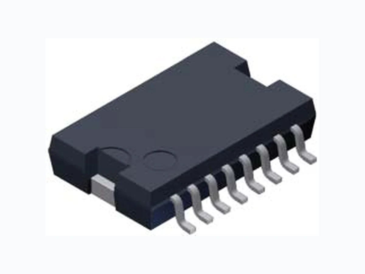
The SPF7302 is a fully protected, single chip full-bridge driver IC for DC brush motor applications. The various protection c i r c u i t s i n t e g r a t e d a r e : o v e r v o l t a g e p r o t e c t i o n ( O V P ) ; overcurrent protection (OCP) with latch, which is adapted to the DMOSFETs in each full bridge; undervoltage lockout (UVLO); open load detection; and overcurrent limitation. The package is a thermally enhanced 16-pin HSOP power package with an exposed thermal pad on the bottom side of the package. Features and Benefits ▪ Supply voltage, VBB , 36 V maximum ▪ Maximum DC current 3 A continuous, 6 A pulsed (1 kHz, duty cycle < 1%, pulse width < 10 μs) ▪ RDS(on) = 300 mΩ maximum, at TJ = 125ºC ▪ Operation modes: forward, reverse, brake (high- or low- side freewheeling current circulation) ▪ Output disable pin (DI pin) ▪ Protections: ▫ Overvoltage protection (OVP), 36 V minimum ▫ Overcurrent protection (OCP), 3 A typical ▫ Overcurrent limitation (OCL), 6 A typical ▫ Externally adjustable delay timer to halt OCL ▫ Thermal shutdown protection (TSD), 151°C minimum ▫ Undervoltage lockout on VBB (UVLO), 4.2 V minimum ▫ Open load detection at startup ▪ Diagnosis output linked to OVP, OCP, TSD, UVLO, and open load detection, at startup and in operation Full Bridge DC Motor Driver Functional Block Diagram Package: 16 pin HSOP with exposed thermal pad and tabs Not to scale Open Circuit Detection Diag OUT1 VBB VBB VBB OUT2 Open Circuit Detection Low-Side Gate Driver High-Side Gate Driver with OVPLow-Side Gate Driver Low-Side OCP Low-Side OCL High-Side OCP High-Side OCL Pre- Regulator IN1 IN2 DI Diagnostics OVP UVLO TSD IN1 IN2 DI High-Side Gate Driver with OVP Diag Diag VREF Diag Diag Diag Diag Diag CP HS1 HS2 LS1 LS2 VBB VBB PGND PGNDLGNDDLY DIAG 28211
Full Bridge DC Motor DriverSPF7302 Selection Guide Part Number Package Packing SPF7302 Thermally enhanced surface mount (HSOP), 16-pin Minimum quantity 1400 pieces All performance characteristics given are typical values for circuit or system baseline design only and are at the nominal operating voltage and an ambient temperature, T A, of 25°C, unless oth er wise stated. Number Name Description
1 LGND Logic GND
2 IN2 Input pin 2
3 IN1 Input pin 1
4 DI Disable pin
5 VBB Supply input voltage
6 VBB Supply input voltage
7 OUT2 Output 2
8 PGND Power GND
9 PGND Power GND
10 OUT1 Output 1
11 VBB Supply input voltage
12 VBB Supply input voltage
13 CP Charge pump capacitor pin
14 DLY Overcurrent limitation delay setting input pin
15 DIAG Diagnostics output pin
16 LGND Logic GND
Allegro MicroSystems, Inc.
115 Northeast Cutoff
Worcester, Massachusetts 01615-0036 U.S.A. Absolute Maximum Ratings at TA = 25°C Characteristic Symbol Notes Rating Unit Supply Voltage V BB –0.3 to 36 V IN1, IN2, DI, and DLY Pin Input Voltage V x –0.3 to 6 V Output Current IO ±3 A IOpeak Continuous: 1 kHz, duty cycle <1%; pulse: < 10 μs± 6 A DIAG Pin Output Voltage V DIAG –0.3 to 6 V DIAG Pin Input Current I DIAG DIAG pin sink current –2 mA CP Pin Voltage V CP –0.3 to 36 V Power Dissipation PD1 With infinite heatsink 39 WPD2 Mounted on glass epoxy PCB, 50 mm × 74 mm × 1.6 mm; 0.5 oz copper (18 μm thick) exposed copper area 4 Junction Temperature T J –40 to 150 ºC Operating Ambient Temperature T A –40 to 105 ºC Storage Temperature T stg 40 to 150 ºC Thermal Resistance, Junction to Case R θJC Mounted on glass epoxy PCB, 50 mm × 74 mm × 1.6 mm; 0.5 oz copper (18 μm thick) exposed copper area 3.2 °C/W Thermal Resistance, Junction to Ambient R θJA 31 °C/W
Full Bridge DC Motor DriverSPF7302 ELECTRICAL CHARACTERISTICS1 valid at TJ = –30°C to 125°C, VBB = 14 V, VDI = 5 V, CCP = 47 nF, RDIAG = 5.1 kΩ, unless otherwise specified Characteristic Symbol Test Conditions Min. Typ. Max. Unit Supply Voltage V BB 6 – 18 V OUTx Pin Leakage Current IleakHS –1 – – mA IleakLS ––1m A DMOSFET On Resistance RDS(ON_1H IOUT = 1 A – – 300 m Ω RDS(ON)_2H IOUT = 3 A – – 300 m Ω RDS(ON)_1L IOUT = 1 A – – 300 m Ω RDS(ON)_2L IOUT = 3 A – – 300 m Ω DMOSFET Body Diode Forward Voltage VF_H1 IOUT1 = 1 A – 1.0 2.0 V VF_H2 IOUT2 = 1 A – 1.0 2.0 V VF_L1 IOUT1 = –1 A – 1.0 2.0 V VF_L2 IOUT2 = –1 A – 1.0 2.0 V Quiescent Current I BB –7–m A Overcurrent Limit (OCL) IOCL_H1 TJ = –40°C to 150°C, IOCL < IOCP ; guaranteed by design 2.0 3.0 4.5 A IOCL_H2 2.0 3.0 4.5 A IOCL_L1 2.0 3.0 4.5 A IOCL_L2 2.0 3.0 4.5 A Overcurrent Protection (OCP) IOCP_H1 TJ = –40°C to 150°C, IOCL < IOCP ; guaranteed by design 4.5 6.0 8.0 A IOCP_H2 4.5 6.0 8.0 A IOCP_L1 4.5 6.0 8.0 A IOCP_L2 4.5 6.0 8.0 A IN1, IN2, DI, and DLY Pin Input Voltage Vx_H 3.0 – 5.3 V Vx_L –0.3 – 1.5 V IN1, IN2, DI, and DLY Pin Input Current Ix_H VDLY = 5 V – 100 200 μA Ix_L VDLY = 0 V –1 – 1 μA DIAG Pin Output Voltage VDIAG_H VCC = 5 V 4.0 – – V VDIAG_L Isink = 2 mA – – 0.4 V DIAG Pin Output Current IDIAG_H VCC = 5 V, DIAG pin source current –250 – – μA IDIAG_L VCC = 5 V, DIAG pin sink current, VDIAG = 2 V – – 3 mA IN1 and IN2 Pin Input Propagation Time tINx_ON Delay from VINx = 2 V→VOUTx × 0.2 – 7 15 μs tINx_OFF Delay from VINx = 1.5 V→VOUTx × 0.8 – 7 15 μs Output Rise Time t rx Delay from VOUTx = 20%→80% points, at IOUTx = 1 A – 0.5 2 μs Output Fall Time t fx Delay from VOUTx = 20%→80% points, at IOUTx = 1 A – 0.5 2 μs Continued on the next page… Allegro MicroSystems, Inc. Worcester, Massachusetts 01615-0036 U.S.A.
Full Bridge DC Motor DriverSPF7302 DLY Pin Threshold Voltage V DLY(th) Overcurrent limitation (OCL) activating voltage 1.4 1.6 1.8 V DLY Pin Sourcing Current2 IDLY 15 30 60 μA UVLO Releasing Voltage V UVLO_OFF – – 5.2 V UVLO Activating Voltage V UVLO_ON 4.2 – – V UVLO Hysteresis V UVLOhys – 0.2 – V OVP Protection Activating Voltage V OVP_ON 36 – 42 V OVP Protection Releasing Voltage V OVP_OFF 32 – 38 V OVP Hysteresis V OVPhys –5– V Thermal Shutdown Activating Temperature3 TTSD_ON Starts at 165°C typical; guaranteed by design 151 165 – ºC Thermal Shutdown Releasing Temperature3 TTSD_OFF Guaranteed by design 136 150 – ºC Thermal Shutdown Hysteresis3 TTSDhys Guaranteed by design – 15 – ºC 1The parameters at TJ = –40ºC to 150ºC are specified by design. The actual production tests are done at 25ºC and 125ºC. 2The individual overcurrent limitation of each DMOSFET is masked during the delay period. Therefore, ensure proper thermal design for dissipating transient temperature increase caused by current during this period. 3TSD (thermal shutdown protection starts at 165ºC typical, and it is specified by design. ELECTRICAL CHARACTERISTICS1 (continued) valid at TJ = –30°C to 125°C, VBB = 14 V, VDI = 5 V, CCP = 47 nF, RDIAG = 5.1 kΩ, unless otherwise specified Characteristic Symbol Test Conditions Min. Typ. Max. Unit Motor Control Truth Table1 Reference Number Status Input Output DMOSFET status DI IN1 IN2 OUT1 OUT2 DIAG HS1 LS1 HS2 LS2
1 Forward rotation 2 H H L H L H ON OFF OFF ON
2 Reverse rotation 2 H L H L H H OFF ON ON OFF
3 Low-side freewheeling H L L L L H OFF ON OFF ON
4 High-side freewheeling H H H H H H ON OFF ON OFF
5 Output disabled L X X Z Z H OFF OFF OFF OFF
6 Overcurrent limitation (OCL) active (HS1) H H X H X H ON OFF X X
7 Overcurrent limitation (OCL) active (HS2) H XHXHHX X O N O F F
8 Overcurrent limitation (OCL) active (LS1) H L X L X H OFF ON X X
9 Overcurrent limitation (OCL) active (LS2) H X L X L H X X OFF ON
10 Overcurrent protection with latch (OCP) active (HS1) H H X Z Z L OFF OFF OFF OFF
11 Overcurrent protection with latch (OCP) active (HS2) H X H Z Z L OFF OFF OFF OFF
12 Overcurrent protection with latch (OCP) active (LS1) H L X Z Z L OFF OFF OFF OFF
13 Overcurrent protection with latch (OCP) active (LS2) H X L Z Z L OFF OFF OFF OFF
14 Undervoltage lockout (UVLO) protection active X X X Z Z L OFF OFF OFF OFF
15 Overvoltage protection (OVP) active X X X X X L XXXX
16 Open load detected at startup L X X X X L OFF OFF OFF OFF
17 Open load detected in operation H X X X X L XXXX
18 Thermal shutdown protection (TSD) active X X X Z Z L OFF OFF OFF OFF
1X is "don't care," Z is high impedance. 2"Forward" and "reverse" only indicate opposite relative direction. Allegro MicroSystems, Inc. Worcester, Massachusetts 01615-0036 U.S.A.
Figure 1. Output Delay Time Figure 2. Output Switching Time Worcester, Massachusetts 01615-0036 U.S.A.
Full Bridge DC Motor DriverSPF7302 1.0 0.8 0.6 0.4 0.2 0123 0123 VBB to OUTx (V) 01 0 2 0 3 0 4 0 High-side DMOSFET RDS(on) Low-side DMOSFET R DS(on) High-side DMOSFET R DS(on) Low-side DMOSFET R DS(on) Quiescent Current versus Supply Voltage CP Pin Voltage versus Supply Voltage TA= –40°C 25°C 150°C TA= –40°C 25°C 150°C VCC= 14 V 6 V 5.5 V TA= –40°C 25°C 150°C 1.0 0.8 0.6 0.4 0.2 0123 0123 1.0 0.8 0.6 0.4 0.2 1.0 0.8 0.6 0.4 0.2 IQ (mA) VBB (V) IOUT (A) VBB to OUTx (V) IOUT (A) OUTx to PGND (V) IOUT (A) OUTx to PGND (V) IOUT (A) 01 0 2 0 3 0 4 0 VBB (V) VCP (V) VCC= 14 V 6 V 5.5 V Characteristic Performance TA = 25°C unless otherwise specified Allegro MicroSystems, Inc. Worcester, Massachusetts 01615-0036 U.S.A.
Full Bridge DC Motor DriverSPF7302 01 3 25 4 01 3 25 4 VOUT1 (V) 0.6 0.5 0.4 0.3 0.2 0.1 0123 DI Pin Threshold Characteristics DIAG Output versus DI SInk Current UVLO Voltage versus Supply Voltage TA= –40°C 25°C 150°C TA= –40°C 25°C 150°C 02 8 641 0 200 100 02 8 641 0 200 100 VDIAG (V) IDI(SINK) (mA) VDI (V) VOUT1 (V) INx Pin Threshold Characteristics DI Pin Current Characteristics INx Pin Current Characteristics VIN (V) VDI (V) VIN (V) IDI(SINK) (μA) IIN(SINK) (μA) 0246 VBB (V) VUVLO (V) TA= –40°C 25°C 150°C Allegro MicroSystems, Inc. Worcester, Massachusetts 01615-0036 U.S.A.
Full Bridge DC Motor DriverSPF7302 25 30 35 45 40 100 140 120 180 160 VDIAG (V) VDIAG (V) DIAG Output Voltage with OVP Activated (IC continues operation) DIAG Output Voltage with TSD Activated (IC stops operation) Output Rise Time, t RX Output Fall Time, tFX VINX = 2 V/div t = 2 μs/div VOUTX = 2 V/div 160 ns VBB (V) Input to Output On Propagation Delay, t INx_ON VINX = 2 V/div t = 2 μs/div VOUTX = 2 V/div VINX = 2 V/div t = 50 ns/div VOUTX = 2 V/div VINX = 2 V/div t = 100 ns/div VOUTX = 2 V/div Input to Output Off Propagation Delay, t INx_OFF TJ (C°) 140 ns 7.9 μs7.8 μs Allegro MicroSystems, Inc. Worcester, Massachusetts 01615-0036 U.S.A.
Full Bridge DC Motor DriverSPF7302 DLY Voltage versus INx Pin Voltage IOUTX = 1 A/div t = 100 μs/div VOUTX = 10 V/div High-side DMOSFET OCL Operation Example Low-side DMOSFET OCL Operation Example High-side DMOSFET OCP Operation Example Low-side DMOSFET OCP Operation Example t = 100 μs/div VOUTX = 10 V/div IOUTX = 2 A/div VINX = 5 V/div t = 10 μs/div VDLY = 0.5 V/div 1.6 V 3.4 A 6.9 A t = 100 μs/div VOUTX = 10 V/div IOUTX = 2 A/div 7.1 A IOUTX = 1 A/div t = 100 μs/div VOUTX = 10 V/div 4.0 A Allegro MicroSystems, Inc. Worcester, Massachusetts 01615-0036 U.S.A.
Figure 4. Open Load Detection Figure 5. Delay to Open Load protection activation versus value of external Figure 3. Behavior of Current Limitation and Overcurrent Protection internal logic circuit and releases the latch. A. During this period, UVLO is activated and DIAG stays low. checked before the time of that event. Worcester, Massachusetts 01615-0036 U.S.A.
by checking the negative potential of the output. arrows marked A in figure 6). During this period, overcurrent protection (OCP) is still active. Figure 6. Open load detection in normal operation Figure 7. DLY pin effect at startup Worcester, Massachusetts 01615-0036 U.S.A.
Full Bridge DC Motor DriverSPF7302
Application Information
Figure 8. Typical application circuit. Recommended components are: Figure 9. Recommended Solder Pad Layout, dimensions in mm Worcester, Massachusetts 01615-0036 U.S.A.
Figure 10. Power Dissipation Derating Curve Figure 12. Test PCB Land Pattern Figure 11. Thermal Resistance versus PCB Copper Area conditions, taking into account actual PCB and load conditions. D OFF is the IN1 and IN2 proportion off (DON + DOFF = 100%). TP is the temperature at the exposed thermal pad of the device. Figure 13. Thermal Performance Worcester, Massachusetts 01615-0036 U.S.A.
Full Bridge DC Motor DriverSPF7302 Package Outline Drawing, 16 Pin HSOP Branding codes (exact appearance at manufacturer discretion): 1st line, type: SPF7302 2nd line, lot: YMDD Where: Y is the last digit of the year of manufacture M is the month ( 1 to 9, O, N, D) DD is the date Package: HSOP-16 Dimensions in millimeters 10.5 ±0.2 12.2 ±0.2 7.50 ±0.2 2 ±0.2 1 ±0.3 1.35 ±0.2 10.5 ±0.3 2.5 ±0.2 0.25 +0.15 –0.05 0.1 0.4 +0.15 –0.05 (3.05) (4.7) 1.27±0.25 Branding Area Exposed thermal pad Tab from exposed thermal pad XXXXXXXX XXXXXXXX View A Enlargement View A(8.89) 0.8) A Leadframe plating Pb-free. Device composition complies with the RoHS directive. Allegro MicroSystems, Inc. Worcester, Massachusetts 01615-0036 U.S.A.
Full Bridge DC Motor DriverSPF7302 WARNING — These devices are designed to be operated at lethal voltages and energy levels. Circuit designs that embody these components must conform with applicable safety requirements. Pre cau tions must be taken to prevent accidental contact with power-line potentials. Do not connect ground ed test equipment. The use of an isolation transformer is recommended during circuit development and breadboarding. Because reliability can be affected adversely by improper storage environments and handling methods, please observe the following cautions. Cautions for Storage
- Ensure that storage conditions comply with the standard temperature (5°C to 35°C) and the standard relative humidity (around 40 to 75%); avoid storage locations that experience extreme changes in temperature or humidity.
- Avoid locations where dust or harmful gases are present and avoid direct sunlight.
- Reinspect for rust on leads and solderability of products that have been stored for a long time. Cautions for Testing and Handling When tests are carried out during inspection testing and other standard test periods, protect the products from power surges from the testing device, shorts between adjacent products, and shorts to the heatsink. Soldering
- When soldering the products, please be sure to minimize the working time, and any soldering iron should be kept at a distance from the body of the product.
- The number of reflow procedures is restricted to two only. Device reliability and appearance are guaranteed within the temperature profile below, after storage conditions of up to 168 hours at T A = 85ºC and RH = 85%. Electrostatic Discharge
- When handling the products, operator must be grounded. Grounded wrist straps worn should have at least 1 MΩ of resistance to ground to prevent shock hazard.
- Workbenches where the products are handled should be grounded and be provided with conductive table and floor mats.
- When using measuring equipment such as a curve tracer, the equipment should be grounded.
- When soldering the products, the head of soldering irons or the solder bath must be grounded in other to prevent leak voltages generated by them from being applied to the products.
- The products should always be stored and transported in our shipping containers or conductive containers, or be wrapped in aluminum foil. 90 to 120s 30s 60s 245 230 200 150 Temperature (ºC) Duration (s) 4 ºC/s Solder Reflow Profile Allegro MicroSystems, Inc.
Worcester, Massachusetts 01615-0036 U.S.A.
Full Bridge DC Motor DriverSPF7302 The products described herein are manufactured in Ja pan by Sanken Electric Co., Ltd. for sale by Allegro MicroSystems, Inc. Sanken and Allegro reserve the right to make, from time to time, such de par tures from the detail spec i fi ca tions as may be re quired to per mit im- prove ments in the per for mance, reliability, or manufacturability of its prod ucts. Therefore, the user is cau tioned to verify that the in for ma tion in this publication is current before placing any order. When using the products described herein, the ap pli ca bil i ty and suit abil i ty of such products for the intended purpose shall be reviewed at the users responsibility. Although Sanken undertakes to enhance the quality and reliability of its prod ucts, the occurrence of failure and defect of semi con duc tor products at a certain rate is in ev i ta ble. Users of Sanken products are requested to take, at their own risk, preventative measures including safety design of the equipment or systems against any possible injury, death, fires or damages to society due to device failure or malfunction. Sanken products listed in this publication are designed and intended for use as components in general-purpose electronic equip ment or apparatus (home ap pli anc es, office equipment, tele com mu ni ca tion equipment, measuring equipment, etc.). Their use in any application requiring radiation hardness assurance (e.g., aero space equipment) is not supported. When considering the use of Sanken products in ap pli ca tions where higher reliability is re quired (transportation equipment and its control systems or equip ment, fire- or burglar-alarm systems, various safety devices, etc.), contact a company sales representative to discuss and obtain written confirmation of your spec i fi ca tions. The use of Sanken products without the written consent of Sanken in applications where ex treme ly high reliability is required (aerospace equip- ment, nuclear power-control stations, life-support systems, etc.) is strictly prohibited. The information in clud ed herein is believed to be accurate and reliable. Ap pli ca tion and operation examples described in this pub li ca tion are given for reference only and Sanken and Allegro assume no re spon si bil i ty for any in fringe ment of in dus tri al property rights, intellectual property rights, or any other rights of Sanken or Allegro or any third party that may result from its use. Anti radioactive ray design is not considered for the products listed herein. Copyright © 2006-2009 Allegro MicroSystems, Inc. Allegro MicroSystems, Inc. Worcester, Massachusetts 01615-0036 U.S.A.