
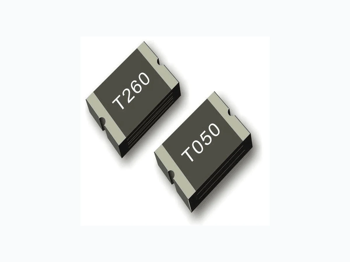
SMD0603P003 LEIDITECH
Document overview
- Manufacturer or author: Provided By www.digicamel.com(FREE DATASHEET DOWNLOAD SITE)
- PDF pages: 6
Technical content
Features: RoHS Compliant & Halogen Free faster tripping, 0603 Dimension, Surface mountable, Solid state Operation Current: 0.03A~0.50A Maximum V oltage: 6V~30Vdc Operating Temperature:-40℃ TO 85℃ Product Dimensions Pig.1 Unit :mm Part Number A B C D E Min Max Min Max Min Max Min Max MAX SMD0603P003 TF 1.45 1.85 0.65 1.05 0.40 0.90 0.15 0.50 0.40 SMD0603P004 TF 1.45 1.85 0.65 1.05 0.40 0.90 0.15 0.50 0.40 SMD0603P005 TF 1.45 1.85 0.65 1.05 0.40 0.75 0.15 0.50 0.40 SMD0603P010 TF 1.45 1.85 0.65 1.05 0.40 0.75 0.15 0.50 0.40 SMD0603P020 TF 1.45 1.85 0.65 1.05 0.40 0.75 0.15 0.50 0.40 SMD0603P025 TF 1.45 1.85 0.65 1.05 0.40 0.75 0.15 0.50 0.40 SMD0603P030 TF 1.45 1.85 0.65 1.05 0.40 0.75 0.15 0.50 0.40 SMD0603P035 TF 1.45 1.85 0.65 1.05 0.40 0.75 0.15 0.50 0.40 SMD0603P040 TF 1.45 1.85 0.65 1.05 0.5 0.15 0.50 0.40 SMD0603P050 TF 1.45 1.85 0.65 1.05 0.5 0.15 0.50 0.40 Terminal pad materials :Tin-Plated Nickle-copper Terminal pad solderability : Meets EIA specification RS 186-9E and ANSI/J-STD-002 Category 3. Positive Thermal Coefficent Diodes SMD0603P003~050 Series Rev : www.leiditech.com 01.06.2018 1/6
Thermal Derating Chart-IH(A) Part number Maximum ambient operating temperatures SMD0603P003 TF 0.042 0.038 0.035 0.03 0.026 0.021 0.018 0.015 0.011 SMD0603P004 TF 0.056 0.05 0.046 0.04 0.034 0.028 0.024 0.02 0.014 SMD0603P005 TF 0.07 0.063 0.058 0.05 0.043 0.035 0.03 0.025 0.018 SMD0603P010 TF 0.14 0.125 0.115 0.1 0.085 0.07 0.06 0.05 0.035 SMD0603P020 TF 0.28 0.25 0.23 0.20 0.17 0.14 0.12 0.10 0.07 SMD0603P025 TF 0.35 0.31 0.29 0.25 0.21 0.18 0.15 0.13 0.09 SMD0603P030 TF 0.42 0.38 0.35 0.30 0.26 0.21 0.18 0.15 0.11 SMD0603P035 TF 0.47 0.44 0.39 0.35 0.30 0.27 0.24 0.20 0.14 SMD0603P040 TF 0.54 0.50 0.45 0.40 0.34 0.31 0.27 0.23 0.16 SMD0603P050 TF 0.67 0.63 0.56 0.50 0.43 0.39 0.34 0.29 0.20 Electrical Characteristic Part Number V max Imax Ihold Itrip P d Maximum time to trip Resistence (Vdc) (A) (A) (A) Max. (W) Current Time Ri min max (A) (Sec) SMD0603P003TF 30.0 20 0.03 0.09 0.50 0.15 1.00 6.0 65.00 SMD0603P004TF 24.0 20 0.04 0.12 0.50 0.2 1.00 4.0 45.00 SMD0603P005TF 24.0 20 0.05 0.15 0.50 0.25 1.00 3.0 35.00 SMD0603P010TF 15.0 40 0.10 0.30 0.50 0.5 1.00 0.9 8.00 SMD0603P020 TF 9.0 0.50 0.50 1.00 0.60 0.55 3.50 SMD0603P025 TF 9.0 0.50 8.0 0.08 0.500 3.00 SMD0603P030 TF 6.0 .30 0.70 0.50 8.0 0.10 0.300 2.00 SMD0603P035 TF 6.0 .35 0.75 0.50 8.0 0.10 0.200 1.400 SMD0603P040 TF 6.0 0.40 0.80 0.50 8.0 0.10 0.20 0.900 SMD0603P050 TF 6.0 0.50 1.00 0.50 8.0 0.10 0.100 0.800 Part Numbering System LM- SMD □□□ leiditech mark Holding current Rating Surface Mount Device
0603 Dimension
SMD0603P003~050 Series Rev : www.leiditech.com 01.06.2018 2/6
Test Procedures And Requirements Test Test Conditions Accept/Reject Criteria Resistance In still air @ 25 R min ≤R≤R max Time to Trip Specified current V max T maximum Time to Trip Hold Current 30min at I H No trip Trip Cycle Life Vmax Imax 100 cycles No arcing or burning Trip Endurance Vmax hours No arcing or burning Physical Characteristics and Environmental Specifications Terminal materials : Tin Plated Nickle copper S oldering zone Meets EIA specification RS 186 9E and ANSI/J STD 002 Category 3. Environmental Specifications Test Conditions Resistance Change Passive aging 85℃,1000hours ± 10% Humidity aging /85%RH. 1000 hours ± 5% T hermal shock MIL-STD-202,Method 107G +85℃/-40℃,20times 30% typical resistance change Solvent Resistance MIL-STD-202,Method 215 no change Vibration ML-STD-883C,Test Condition A No chage Electrical Specifications: Ihold = Hold Current. Maximum current device will not trip in 25° C still air. Itrip = Trip Current. Minimum current at which the device will always trip in 25° C still air. Vmax = Maximum operating voltage device can withstand without damage at rated current (Imax). Imax = Maximum fault current device can withstand without damage at rated voltage (Vmax). Pd=Maximum power dissipation when device is in the tripped state in 25° C still air environment at rated voltage. Rimin/max = Minimum/Maximum device resistance prior to tripping at 25° C. R1max = Maximum device resistance is measured one hour post reflow. SMD0603P003~050 Series Rev : www.leiditech.com 01.06.2018 3/6
Recommended pad layout (mm) Solder reflow conditions
- Recommended reflow methods: IR, vapor phase oven, hot air oven, N2 environment for lead-free.
- Devices are not designed to be wave soldered to the bottom side of the board.
- Recommended maximum paste thickness is 0.25mm (0.010inch).
- Devices can be cleaned using standard industry methods and solvents. SMD0603P003~050 Series
- Soldering temprature profile meets RoHs leadfree process. Notes: If reflow temperatures exceed the recommended profile, devices may not meet the performance requirements Rev : www.leiditech.com 01.06.2018 4/6
Tape Specification And Reel Dimensions Coverning Specifications EIA 481-1(Unit:mm) W ± 0. P 4.0 ± 0.10 P1 4.0± 0.10 P2 2.0 ± 0.05 A 0.95 ± 0.10 B0 1.85 ± 0. D0 1.55± 0.05 F 3.50± 0.05 E1 1.75 ± 0.10 T 0.20± 0. Leader min. 390 Trailer min. 160 Reel Dimensions A 178± 1.0 N 59± 1 W 8.5+1.0/ 0.2 W 12.0± 1 SMD0603P003~050 Series Rev : www.leiditech.com 01.06.2018 5/6
The maximum ambient temperature shall not exceed 38℃. Storage temperatures higher than 38℃ could result in the deformation of packaging materials. The maximum relative humidity recommended for storage is 60%. High humidity with high temperature can accelerate the oxidation of the solder plating on the termination and reduce the solderability of the components. Sealed plastic bags with desiccant shall be used to reduce the oxidation of the termination and shall only be opened prior to use. The products shall not be stored in areas where harmful gases containing sulfur or chlorine are present WARNING
- Use PPTC beyond the maximum ratings or improper use may result in device damage and possible electrical arcing and flame.
- PPTC are intended for protection against occasional over current or over temperature fault conditions and should not be used when repeated fault conditions or prolonged trip events are anticipated.
- Device performance can be impacted negatively if devices are handled in a manner inconsistent with recommended electronic, thermal, and mechanical procedures for electronic components.
- Use PPTC with a large inductance in circuit will generate a circuit voltage (L di/dt) above the rated voltage of the PPTC.
- Avoid impact PPTC device its thermal expansion like placed under pressure or installed in limited space.
- Contamination of the PPTC material with certain silicon based oils or some aggressive solvents can adversely impact the performance of the devices.PPTC SMD can be cleaned by standard methods.
- Requests that customers comply with our recommended solder pad layouts and recommended reflow profile. Improper board layouts or reflow profilecould negatively impact solderability performance of our devices. SMD0603P003~050 Series Shanghai Leiditech Electronic Co.,Ltd Email: sale1@leiditech.com Tel : +86- 021 50828806 Fax : +86- 021 50477059 Rev : www.leiditech.com 01.06.2018 6/6