
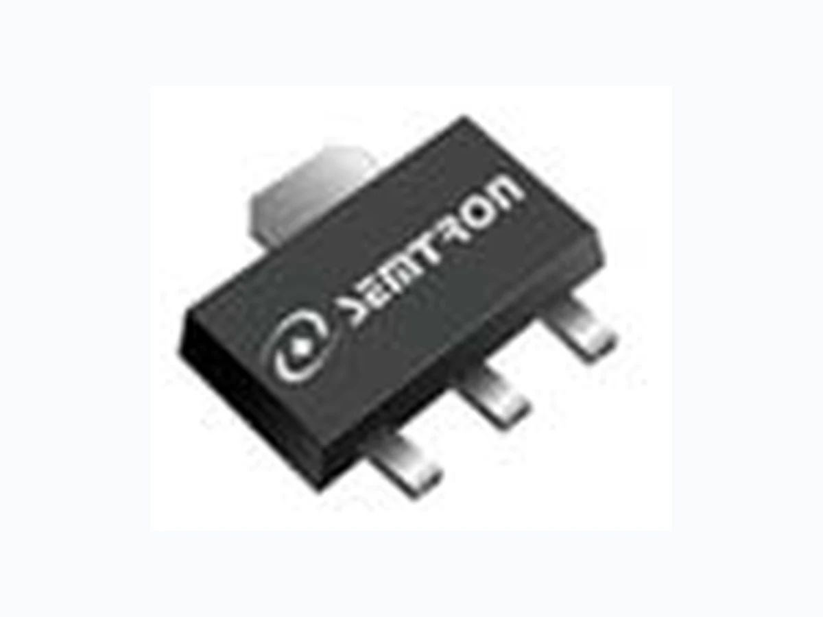
SMC3535AK SEMTRON
Document overview
- Manufacturer or author: Provided By www.digicamel.com(free datasheet download site)
- PDF pages: 5
Technical content
SMC3535AK Rev.A2 Copyright © Semtron Microtech Corp. www.semtron-micro.com ■ABSOLUTE MAXIMUM RATINGS (TA=25°C Unless otherwise noted ) Symbol Parameter Rating Units VDSS Drain-Source Voltage -30 V VGSS Gate-Source Voltage ±12 V ID Continuous Drain Current TA=25°C -6.6 A TA=70°C -5.3 A IDM Pulsed Drain Current B -26.4 A PD Power Dissipation A TA=25°C 3.6 W TA=70°C 2.3 W TJ Operation Junction Temperature -55/150 °C TSTG Storage Temperature Range -55/150 °C ■THERMAL RESISTANCE Symbol Parameter Typ Max Units RθJA Thermal Resistance Junction to Ambient A t≦10s 35 °C/WThermal Resistance Junction to Ambient AC Steady-State 70 ■DESCRIPTION SMC3535AK is the P-Channel logic enhancement mode power field effect transistor is produced using high cell density. advanced trench technology to provide excellent R DS(ON), low gate charge and operation gate as 2.5V. This device is suitable for use as a load switch or other general applications. ■PART NUMBER INFORMATION Single P-Channel MOSFET SMC 3535A K - TR G a b c d e a : Company name. b : Product Serial number. c : Package code K:SOT-89 d : Handling code TR:Tape&Reel e : Green produce code G:RoHS Compliant ■FEATURES VDS=-30V, ID=-6.6A RDS(ON)=45mΩ(Typ.)@VGS=-10V RDS(ON)=52mΩ(Typ.)@VGS=-4.5V RDS(ON)=68mΩ(Typ.)@VGS=-2.5V ◆Fast switch ◆Low gate charge ◆High power and current handling capability ■APPLICATIONS ◆Portable Equipment ◆Power Management ◆Load Switch SOT-89 S G D S D G
SMC3535AK Rev.A2 Copyright © Semtron Microtech Corp. www.semtron-micro.com ■ELECTRICAL CHARACTERISTICS(TA=25°C Unless otherwise noted ) Symbol Parameter Condition Min Typ Max Unit Static Parameters BVDSS Drain-Source Breakdown Voltage VGS=0V, ID=-250μA -30 V VGS(th) Gate Threshold Voltage V DS=VGS, ID=-250μA -0.5 -0.7 -1 V IGSS Gate Leakage Current V DS=0V, VGS=±12V ±100 nA IDSS Zero Gate Voltage Drain Current VDS=-30V, VGS=0V, TJ=25°C -1 μAVDS=-24V, VGS=0V, TJ=75°C -10 RDS(ON) Drain-source On-Resistance D VGS=-10V, ID=-6.6A VGS=-4.5V, ID=-4A VGS=-2.5V, ID=-3A mΩ Gfs Forward Transconductance V DS=-10V, ID=-5A 6 S Diode Characteristics VSD Diode Forward Voltage D I S=-1A, VGS=0V -1 V IS Diode Continuous Forward Current -3.3 A Dynamic and Switching Parameters E Qg Total Gate Charge VDS=-15V, VGS=-10V,ID=-5A 17.4 24.4 nCQg Total Gate Charge (4.5V) 8.5 11.5 Qgs Gate-Source Charge 2.1 2.8 Qgd Gate-Drain Charge 1.5 2.1 Ciss Input Capacitance VDS=-15V, VGS=0V, f=1MHz 805 pF Coss Output Capacitance 78 Crss Reverse Transfer Capacitance 48 td(on) Turn-On Time VDD=-15V, VGEN=-10V, RG=6Ω, ID=-1A 5.6 11 nStr 21 40 td(off) Turn-Off Time 43.9 83 tf 10.8 21 Note: Absolute maximum ratings are those values beyond which the device could be permanently damaged. A. Surface mounted on FR4 board using 1 in 2 pad size. B. Pulsed width limited by maximum junction temperature, T J(MAX)=150°C (initial temperature TJ=25°C). C. Using ≤ 10s junction-to-ambient thermal resistance is base on TJ(MAX)=150°C. D. Pulse test width ≤300μs and duty cycle ≤ 2%. E. Guaranteed by design, not s ubject to production testing. The products and product specifications contained herein are subject to change without notice to improve performance characteristics. Consult us, or our representatives before use, to confirm that the information in this datasheet is up to date We assume no responsibility for any infringement of patents, patent rights, or other rights arising from the use of any information and circuitry in this datasheet.
SMC3535AK Rev.A2 Copyright © Semtron Microtech Corp. www.semtron-micro.com ■TYPICAL CHARACTERISTICS 012345 ‐ID‐Drain Current(A) ‐VDS‐Drain Source Voltage(V) Output Characteristics VGS=‐3V VGS=‐2.5V VGS=‐1.8V 100 02468 1 0 RDS(ON)(mΩ) ‐ID‐Drain Current(A) Drain‐Source On Resistance VGS=‐4.5V VGS=‐10V VGS=‐2.5V TA=25°C 0369 1 2 1 5 1 8 ‐VGS(V) Qg‐Gate Charge(nC) Gate Charge 200 400 600 800 1000 1200 0 5 10 15 20 25 30 Capacitance(pF) ‐VDS‐Drain Source Voltage(V) Capacitance Ciss Coss Crss 0.4 0.5 0.6 0.7 0.8 0.9 1.1 1.2 1.3 1.4 ‐50 ‐25 0 25 50 75 100 125 150 Normalized Threshold Voltage TJ‐Junction Temperature(°C) Gate Threshold Voltage 0.5 1.5 2.5 3.5 0 2 55 07 5 1 0 0 1 2 5 1 5 0 Ptot‐Power(W) TJ‐Junction Temperature(°C) Power Dissipation TA=25°C VDS=‐15V ID=‐5A
SMC3535AK Rev.A2 Copyright © Semtron Microtech Corp. www.semtron-micro.com ■TYPICAL CHARACTERISTICS 0.7 0.8 0.9 1.1 1.2 1.3 1.4 1.5 1.6 ‐50 ‐25 0 25 50 75 100 125 150 Normalized On Resistance TJ‐Junction Temperature(°C) RDS(ON) vs Junction Temperature 25 50 75 100 125 150 ‐ID‐Drain Current(A) TJ‐Junction Temperature(°C) Drain Current vs TJ TA=25°C 0.01 0.1 100 0.01 0.1 1 10 100 -ID (A) Maximum Safe Operation Area ‐VDS Voltage (V) 1ms 0.001 0.01 0.1 0.0001 0.001 0.01 0.1 1 10 100 1000 Normalized Transient Thermal Resistance Square Wave Pulse Duration(Sec) Thermal Transient Impedance Duty=0.5 0.2 0.1 0.05 0.02 0.01 Single Pulse Qgd Qg ‐VGS Qgs V Charge Gate Chrge Waveform VGS VDS 10% 90% Td(on) Tr Switching Time Waveform Ton Toff Td(off) Tf TA=25°C 100ms 100µs DC 10ms Duty Cycle, D=t1/t2
SMC3535AK Rev.A2 Copyright © Semtron Microtech Corp. www.semtron-micro.com ■SOT-89 PACKAGE DIMENSIONS Symbol Dimensions In Millimeters Dimensions In Inches Min. Max. Min. Max. A 1.440 1.540 0.567 0.606 b 0.350 0.450 0.138 0.177 b1 0.450 0.550 0.177 0.217 c 0.350 0.450 0.138 0.177 D 4.450 4.550 1.752 0.791 D1 1.650 1.750 0.650 0.689 E 2.450 2.550 0.965 1.004 E1 3.950 4.250 1.555 1.673 e 1.450 1.550 0.571 0.610 e1 2.900 3.100 1.142 1.220 L 0.900 1.200 0.354 0.472 θ 2° 10° 2° 10° c b D e E A