

 Download PDF
SM9233 SMI
Document overview
- PDF pages: 18
Technical content
Page 1

DESCRIPTION
The SM923x series are digital, ultra-low pressure sensors offering state-of-the-art MEMS pressure transducer technology and CMOS mixed signal processing technology to produce a digital, fully conditioned, multi-order pressure and temperature compensated sensor in JEDEC standard SOIC-16 package with a dual vertical porting option. It is available in a gauge pressure configuration.
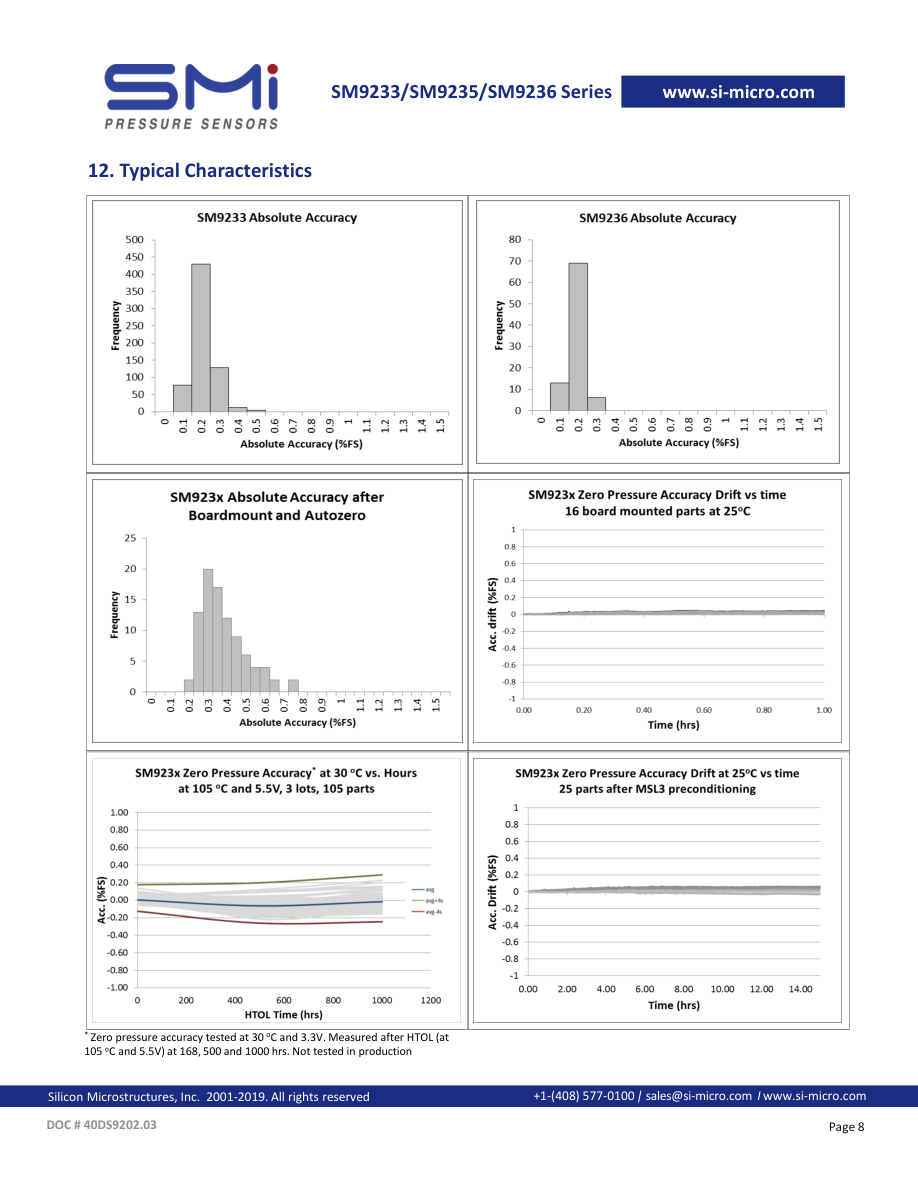
The total accuracy after board mount and system level autozero is less than 1%FS. The excellent warmup behavior and long term stability further assures its expected performance over the life of the part.
Gauge Pressure Sensors
FEATURES
- Pressure ranges: 250 up to 600 Pa Gauge
- Accuracy after Autozero: < 1%FS
- 16 bit I2C Digital interface
- Pressure calibrated and temperature compensated output
- Compensated temperature range: -20 to 85oC
Combining the pressure sensor with a signal-conditioning ASIC in a single package simplifies the use of advanced silicon micro-machined pressure sensors. The pressure sensor can be mounted directly on a standard printed circuit board and a high level, calibrated pressure signal can be acquired from the digital interface. This eliminates the need for additional circuitry, such as a compensation network or microcontroller containing a custom correction algorithm.
The SM9233/SM9235/SM9236 are shipped in sticks or tape & reel.
| Medical | Industrial |
| Sleep Apnea | HVAC / VAV |
| CPAP | Airflow Measurement |
| Ventilators | Pressure Transmitters |
| Gas Flow Instrumentation | Pneumatic Gauges |
| Air Flow Monitors | Pressure Switches |
| Life Sciences | Safety Cabinets |
| Gas Flow Instrumentation |
Page 1
Page 2
1. Absolute Maximum Ratings
All parameters are specified at Vdd = 3.3 V supply voltage at 25oC, unless otherwise noted.
| No. | Characteristic | Symbol | Minimum | Maximum | Units |
|---|---|---|---|---|---|
| 1 | Supply Voltage | V DD | 3.0 | 5.5 | V |
| 2 | Digital IO Voltage | V IO,DIG | -0.3 | VDD+0.3 | V |
| 3 | Max. Digital IO Current (DC) | I IO,DIG | -10 | +10 | mA |
| 4 | Storage Temperature(a,b) | T STG | -40 | +125 | °C |
| 5 | Proof Pressure (a, c) | P Proof | 7 (1.0) | kPa (PSI) | |
| 6 | Burst Pressure (a, d) | P Burst | 20 (2.9) | kPa (PSI) |
Notes:
a. Tested on a sample basis. b. Clean, dry air compatible with wetted materials. Wetted materials include silicon, glass, RTV (silicone), gold, aluminum, copper, nickel, palladium, epoxy, stainless steel and plastic (mold compound). c. Proof pressure is defined as the maximum pressure to which the device can be taken and still perform within specifications after returning to the operating pressure range. d. Burst pressure is the pressure at which the device suffers catastrophic failure resulting in pressure loss through the device.
- ESD
| No. | Description | Symbol | Minimum | Maximum | Units |
|---|---|---|---|---|---|
| 2.1 | ESD HBM Protection at all Pins | V ESD(HBM) | -2 | 2 | kV |
3. External Components
| No. | Description | Symbol | Min. | Typ. | Max. | Units |
|---|---|---|---|---|---|---|
| 1 | Supply bypass capacitor* | C VDD | 100 | nF | ||
| 2 | I2C Data and clock pull up resistors* | R P | 4.7 | kOhm |
\* Not tested in production
4. Calibrated Pressure Ranges
| Calibrated Pressure Ranges | |||
| No. | Device Type | P (Pa) MIN | P (Pa) MAX |
| 1 | SM9233 – 250 Gauge | 0 | +250 |
| 2 | SM9235 –300 Gauge | 0 | +300 |
| 3 | SM9236 –600 Gauge | 0 | +600 |
Page 2
Page 3
5. Recommended Operating Conditions
The recommended operating conditions must not be exceeded in order to ensure proper functionality of the device. All parameters specified in the following sections refer to these recommended operating conditions unless stated otherwise.
| No. | Description | Symbol | Min. | Typ. | Max. | Units |
|---|---|---|---|---|---|---|
| 1 | Supply Voltage | V VDD | 3.0 | 3.3 | 5.5 | V |
| 2 | Low level input voltage at SDA, SCL | V IN,I2C,lo | -0.3 | 0.9 | V | |
| 3 | High level input voltage at SDA, SCL | V IN,I2C,hi | 0.8 * V VDD | V +0.3 VDD | V | |
| 4 | Compensated Temperature (b) | T COMP | -20 | +85 | °C | |
| 5 | Operating Temperature | T A | -20 | 85 | °C |
Notes:
b. Clean, dry air compatible with wetted materials.
6. OPERATING CHARACTERISTICS TABLE
All parameters are specified at Vdd = 3.3 V or 5 V DC supply voltage (as per P/N counter in table 10) at 25oC, unless otherwise noted.
| No. | Characteristic | Symbol | Minimum | Typical | Maximum | Units | |
|---|---|---|---|---|---|---|---|
| 1 | Supply Current at 3.3V (e) | I VDD3p3 | 3.3 | 4.1 | mA | ||
| Supply Current at 5.0V (e) | I VDD5p0 | 3.9 | 5.0 | ||||
| 2 | Digital Pressure Output @ P MIN | OUT MIN | -26,215 | Counts | |||
| 3 | Digital Pressure Output @ P MAX | OUT MAX | +26,214 | Counts | |||
| 4 | Digital Full Scale Span | FS | 52,429 | Counts | |||
| 5 | Resolution (Digital Output) | 16 | Bits | ||||
| 6 | Update Rate | 2000 | Hz | ||||
| 7 | Digital AZ Output Accuracy (f, g, h) | SM9233 – 250 Gauge | ACC AZ | -1.25 | ± 0.25 | 1.25 | %FS |
| SM9235 – 300 Gauge | -1.0 | ± 0.2 | 1.0 | %FS | |||
| SM9236 – 600 Gauge | -1.0 | ± 0.1 | 1.0 | %FS | |||
| 8 | Digital Output Accuracy (f) | SM9233 – 250 Gauge | ACC | -2.75 | ± 0.5 | 2.75 | %FS |
| SM9235 – 300 Gauge | -2.3 | ± 0.4 | 2.3 | ||||
| SM9236 – 600 Gauge | -1.25 | ± 0.3 | 1.25 | %FS | |||
| 9 | Bandwidth | BW | 20 | Hz | |||
| 10 | Position Sensitivity | S G | 0.1 | %FS/g | |||
| 11 | Power-up time* | From supply VDD > 3.0 V to output settled to 63% of final value | t UP | 18 | ms | ||
| 12 | Step response time* | Pressure step response; settled to 63% of final value | t RESP | 18 | ms | ||
| 13 | Step response settling time* | Pressure step response; output settled to full accuracy | t SETTLE | 45 | ms | ||
\* Not tested in production
Notes:
e. Supply current given for continuous operation. Device can be set to sleep mode with significantly lower power consumption. Refer to section 11 for details. f. The accuracy specification applies over all operating conditions in dry clean air. This specification includes the combination of linearity, repeatability, and hysteresis errors over pressure, temperature, and 3.3 V supply voltage. g. Based on system level autozero at 25 oC after board mount or solder reflow. h. Based on sample testing during initial product qualification, not tested in production.
Page 3
Page 4

| No. | Description | Condition | Symbol | Min. | Typ. | Max. | Units |
|---|---|---|---|---|---|---|---|
| 1 | SDA output low voltage* | I = 3 mA SDA | V SDA,OL | 0 | 0.4 | V | |
| 2 | Low-to-High transition threshold* | pins SA0, SCL | V SDA,LH | 0.5 | 0.6 | 0.7 | VDD |
| 3 | High-to-Low transition threshold* | pins SA0, SCL | V SDA,HL | 0.3 | 0.4 | 0.5 | VDD |
| 4 | I2C clock frequency* | f SCL | 400 | kHz | |||
| 5 | Bus free time between a START and STOP condition* | t BUSF | 1300 | ns | |||
| 6 | Clock low time* | t LO | 1300 | ns | |||
| 7 | Clock high time* | t HI | 600 | ns | |||
| 8 | START condition hold time* | t SH | 100 | ns | |||
| 9 | Data setup time* | t SU | 100 | ns | |||
| 10 | Data hold time* | t H | 0 | ns | |||
| 11 | Setup time for repeated START condition* | t RSH | 600 | ns | |||
| 12 | Setup time for STOP condition* | t PSU | 600 | ns | |||
| 13 | Rise time of SDA and SCL signals* | t R | 300 | ns | |||
| 14 | Fall time of SDA and SCL signals* | t F | 300 | ns |

Page 5
9. Package Reference
SOIC-16 (C) Vertical Package Dimensions
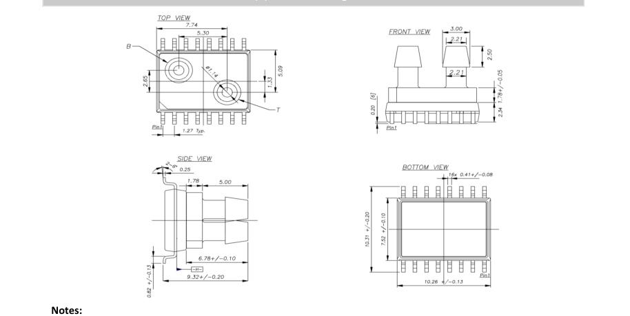
- All dimensions in units of [mm]
- Moisture Sensitivity Level (MSL): Level 3
- Clean, dry air compatible with wetted materials. Wetted materials include : Wetted materials include silicon, glass, RTV (silicone), gold, aluminum, copper, epoxy and mold compound.
- Tolerance on all dimensions ±0.13 mm unless otherwise specified.
- [B] is tube connected to bottom side of sensor die.
- [T] is tube connected to top side of sensor die. Topside pressure is positive pressure. An increase in topside pressure will result in an increase in sensor output
- Bottom plate is stainless steel
- Robust JEDEC SOIC-16 package for automated assembly
- Manufactured according to ISO9001 , ISO14001 and ISO/TS 16949 standards
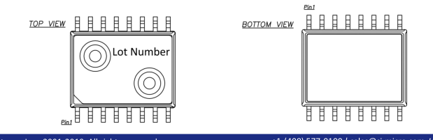
Lot Number Identification
Page 5
Page 6
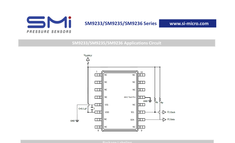
| Package Labeling | |
| Pin No. | Pin Function |
| 1 | NC (No Connect) |
| 2 | NC |
| 3 | NC |
| 4 | NC |
| 5 | VSS |
| 6 | VDD |
| 7 | NC |
| 8 | NC |
| 9 | NC |
| 10 | SDA |
| 11 | SCL |
| 12 | NC |
| 13 | GND (ASIC Test Pin) |
| 14 | NC |
| 15 | NC |
| 16 | NC |

Page 7

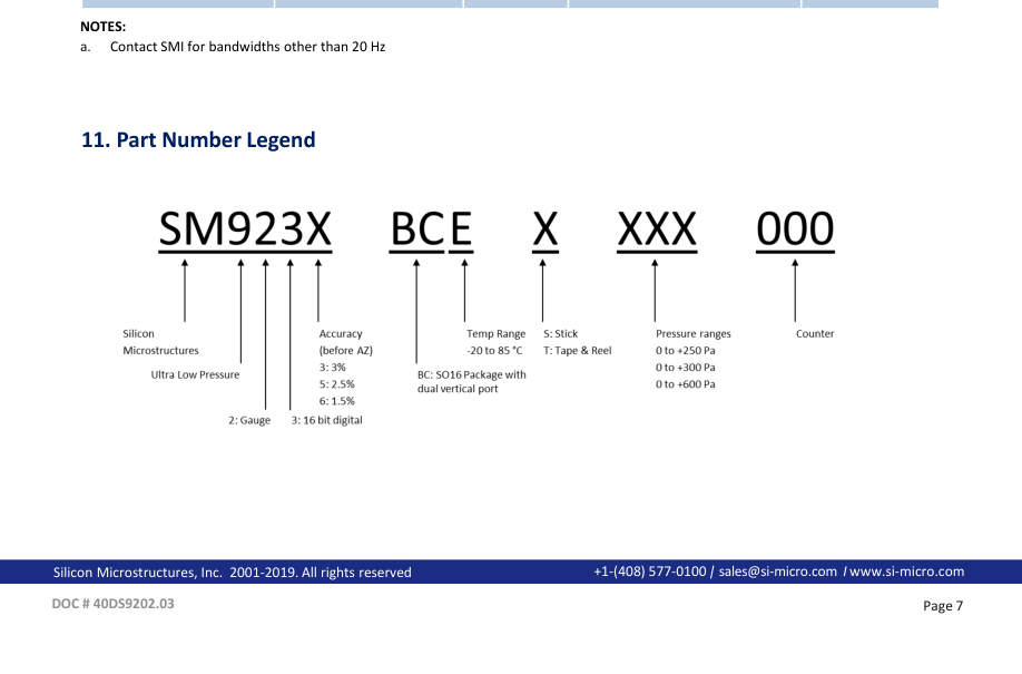
| Part Number | Pressure Range | Voltage | Shipping | Comment |
|---|---|---|---|---|
| SM9233-BCE-S-250-000 | 0 to +250 Pa | 3.3 V | Sticks (45 parts/stick) | Bandwidth 20Hz a |
| Tape and Reel (350 parts/reel) | ||||
| SM9233-BCE-T-250-000 | ||||
| SM9235-BCE-S-300-000 | 0 to +300 Pa | 3.3 V | Sticks (45 parts/stick) | Bandwidth 20Hz a |
| SM9235-BCE-T-300-000 | Tape and Reel (350 parts/reel) | |||
| SM9236-BCE-S-600-000 | 0 to +600 Pa | 3.3 V | Sticks (45 parts/stick) | Bandwidth 20Hz a |
| Tape and Reel (350 parts/reel) | ||||
| SM9236-BCE-T-600-000 | ||||
| SM9233-BCE-S-250-002 | 0 to +250 Pa | 5.0 V | Sticks (45 parts/stick) | Bandwidth 20Hz a |
| Tape and Reel (350 parts/reel) | ||||
| SM9233-BCE-T-250-002 | ||||
| SM9235-BCE-S-300-002 | 0 to +300 Pa | 5.0 V | Sticks (45 parts/stick) | Bandwidth 20Hz a |
| SM9235-BCE-T-300-002 | Tape and Reel (350 parts/reel) | |||
| SM9236-BCE-S-600-002 | 0 to +600 Pa | 5.0 V | Sticks (45 parts/stick) | Bandwidth 20Hz a |
| Tape and Reel (350 parts/reel) | ||||
| SM9236-BCE-T-600-002 |
Page 8
Page 9
13. Functional Description
13.1 Overview
The SM9x3x series is a high precision, factory calibrated Gauge pressure sensor for ultra low pressure measurements. It combines a low pressure MEMS die with a 16 bit ASIC, utilizing DSP for multi dimensional polynomial error correction. The calibrated pressure output data is available via digital data interface (I2C). Status information on the sensor integrity and unique serial number are accessible via this digital interface.
13.2 Global Sensor Parameters
13.2.1 Digital Pressure Transfer Function In general digital output data is available with a word length of 16 bit. The numeric representation is always as 2's complement, which results in a range of:
0 ... +32767 counts (positive range, or 0000h ... 7FFFh) -32768 ... -1 counts (negative range, or 8000h ... FFFFh)
The pressure sensor device is calibrated in the end-of-line production test over the specified Pmin to Pmax pressure range (see Section 4). The output code at Pmin is nominally -26,215 and at Pmax it is nominally 26,214. This allows the sensor to still operate monotically outside its nominal range till the maximum (or minimum) counts are reached. An example for a 250 Gauge SM9233-BCE-S-250-000 is given in the
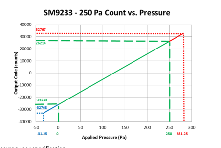
graph below
Green: Accuracy per specification Red and Blue: Outside specification, but expect monotonic behavior till maximum (or minimum) code is reached
13.2.2 Conversion from counts to pressure The digital output count gives a signed 16 bit value for pressure and to convert the count to a pressure percent reading, p%FS, (in % full scale pressure) the following equation can be used
The equation below converts p%FS to actual calibrated pressure units pp-unit with pmin and pmax as specified in section 4
Page 9
Page 10
13.2.4 Digital Temperature Transfer Function An internal temperature sensor measures the chip temperature. The temperature characteristic is linear and is described by the following equation:
DT = b1 \* TA + b0
The temperature transfer function parameters are as follows:
| Temperature | Digital Output | Sensitivity / Offset | ||||
| Symbol | Temperature [°C] | Symbol | Value [counts ] | Symbol | Value | Unit |
| T A,1 | -40 | D T,OUT,1 | -32768 | b 1 | 397.2 | counts/°C |
| T A,2 | 125 | D T,OUT,2 | 32767 | b 0 | -16881 | counts |
The typical temperature accuracy at 30 °C is within ± 2 °C.
13.3 Voltage Supply
The device is supplied from pin VDD, typically 3.3 V, but it can operate as high as 5 V. From this supply input several internal voltage regulators are generating stabilized voltage levels for analog and digital circuit sections. The different internal voltages are monitored by power-OK diagnostic circuitry. Also a stabilized voltage for the resistive MEMS pressure sensor is derived from VDD.
The digital data interface allows to set it into Sleep Mode using a specific command (Enter Sleep Mode), which ensures very low consumption (IVDD,SM) of typically less than 10 µA. Of course, in Sleep Mode no pressure data is acquired.
For the I2C command to send the sensor into Sleep Mode see 13.6. To wake-up the sensor to normal operation, the clock input SCL shall be toggled (a rising edge at SCL will wake-up the device).
13.4 Diagnosis Functions
13.4.1 MEMS Sensor Bridge Diagnostics Internal errors of the MEMS pressure sensor are detected and the STATUS registers can be read via the digital I2C interface.
Bridge Diagnostics An integrated bridge diagnostic circuit supervises the resistive pressure sensor to detect any of the faults as follows:
- Sensor faults:
- Short of any of the four bridge resistors of the pressure sensor
- Interruption of any of the four of bridge resistors
- Wiring faults:
- Open connection of any of the bridge supply or signals
- Wrong connection of any sensor bridge terminal to either ground or bridge supply
The MEMS sensor bridge diagnostics are active permanently (true background diagnostics) and in case of an error the bridge check fail event is indicated by setting the bit bc_fail in the internal STATUS register.
Bridge Supply Diagnostics Another diagnostic function checks if the supply to the sensor bridge is in its specified range. Here, in case of a supply error the bit bs_fail in the STATUS register will be set.
13.4.2 Configuration Memory Check The integrity of data stored in the embedded NVM used as the configuration memory (calibration parameters, device configuration, device ID, etc.) is checked at power-up of the component by calculation of a check sum (CRC). If a check sum error is detected no reliable pressure calculation is possible. Therefore, the sensor remains in idle state, i.e. no pressure data transferred to the output registers DSP_T and DSP_S. In this case the bits STATUS.dsp_s_up and dsp_t_up will never be set.
Page 10
Page 11
13.5 I2C Interface
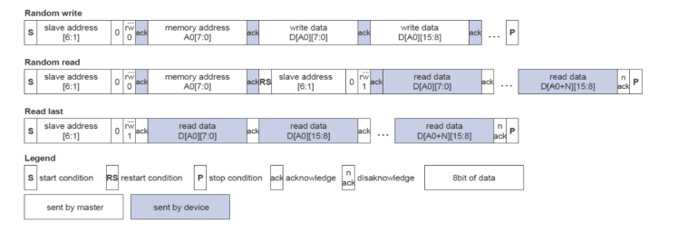
The SM9x3x features an I2C slave interface. This interface provides direct access to registers of the memory of the SM9x3x sensor. An external I2C master (e.g. a microcontroller) can read from and write to memory addresses (registers) of the device using the following commands:
- Random write: Sets a memory address and writes data to consecutive memory addresses of the device starting at the set memory address.
- Random read: Sets a memory address and reads data from consecutive memory addresses of the device starting at the set memory address.
- Read last: Reads data from the device starting at the last memory address set by the master. This facilitates repeated reading of the same memory addresses without transmitting a memory address first.
All reads/writes must start at word aligned addresses (i.e. LSB of memory address equals 0) and read/write an even number of bytes.
I2C Interface Timing Diagram:
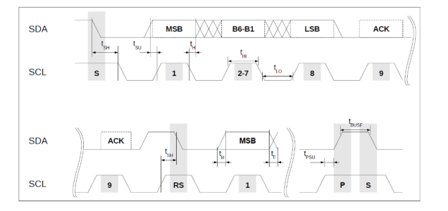
13.5.1 I2C Command Format The SM9x3x-Sensor uses a standard 7-bit I2C slave address field. The LSB of the slave address specifies the frame type used to perform read and write operations. For LSB = 0 the protocol is compatible to standard I2C EEPROMs, for LSB = 1 the protocol is extended by a CRC protection. Thus, each device occupies two I2C addresses: even addresses are for standard EEPROM compatible protocols and odd addresses are for CRC protected protocols. Unprotected and CRC protected frames can be interleaved.
The two different frame types - standard EEPROM (without CRC) or CRC protected - are shown in the next two figures.
Page 11
Page 12
I2C Read / Write Commands - Standard EEPROM compatible protocol:
I2C Read / Write Commands - CRC protected protocol:
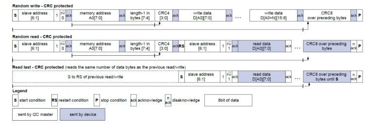
The memory address field sets the byte address of the first memory location to be read from or written to. Only 16-bit-word aligned reads/writes are supported, i.e. the LSB of memory address has to be zero always. The read/write data is transferred MSB first, low byte before high byte. The length field (bits[7:4]) required for CRC protected frames specifies the number of data bytes to be transferred decremented by one, i.e. a value of 0001b corresponds to two bytes. All frames must transfer an even number of bytes. The maximum length for CRC protected read/write frames is 16/4 bytes. For unprotected frames the length is unlimited.
Page 12
Page 13
The CRC4 and CRC8 for redundancy check are computed in the same bit and byte order as the transmission over the bus. The polynomials employed are:
- CRC4: polynomial 0x03; initialization value: 0x0F
- CRC8: polynomial 0xD5; initialization value: 0xFF
If a CRC errors occurs, then the event bit com_crc_error in the STATUS register will be set.
13.5.2 I2C Command Examples For all examples below the 7-bit device slave address used is 0x6C for unprotected commands, and 0x6D for CRC protected commands, respectively.
The command sequence following describes an unprotected Read command (without CRC) of 3 subsequent 16-bit words starting at memory address 0x2E to read the corrected IC temperature, corrected pressure signal, and (synchronized) status bits of the sensor.
Random Read:
| Byte # | 0 | 1 | 2 | 3 | 4 | 5 | 6 | 7 | 8 |
| SBM (sent by master) | 0xD8 | 0x2E | 0xD9 | ||||||
| SBM comment | slave address 6C + LSB = 0 for Write | memory address | slave address 6C + LSB = 1 for Read | ||||||
| SBS (sent by sensor) | 0xF2 | 0x7D | 0xEA | 0x82 | 0x1E | 0x00 | |||
| SBS comment | DSP_T (Lo-Byte) ad. 0x2E | DSP_T (Hi-Byte) | DSP_S (Lo-Byte) ad. 0x30 | DSP_S (Hi-Byte) | sync‘ed Status (b7 - b0) ad. 0x32 | sync‘ed Status (b15 - b8) |
The following sequence writes one 16-bit word to address 0x22. This will copy 0x6C32 into the command register CMD to move the component to Sleep Mode.
Random Write:
| Byte # | 0 | 1 | 2 | 3 |
| SBM (sent by master) | 0xD8 | 0x22 | 0x32 | 0x6C |
| SBM comment | slave address 6C + LSB = 0 for Write | memory address | Lo-Byte written to CMD[7:0] | Hi-Byte written to CMD[15:8] |
| SBS (sent by sensor) | ||||
| SBS comment |
Page 13
Page 14

| Byte # | 0 | 1 | 2 | 3 | 4 | 5 | 6 | 7 | 8 | 9 | 10 |
| SBM (sent by master) | 0xDA | 0x2E | 0x5B | 0xDB | |||||||
| SBM comment | slave address 6D + LSB = 0 for Write | memory address | 3: length = 4Byte B: CRC4 | slave address 6D + LSB = 1 for Read | |||||||
| SBS (sent by sensor) | 0xF2 | 0x7D | 0xEA | 0x82 | 0x1E | 0x00 | 0x65 | ||||
| SBS comment | DSP_T (Lo-Byte) ad. 0x2E | DSP_T (Hi-Byte) | DSP_S (Lo-Byte) ad. 0x30 | DSP_S (Hi-Byte) | sync‘ed Status (b7 - b0) ad. 0x32 | sync‘ed Status (b15 - b8) | CRC8 (calc'd) |

| Byte # | 0 | 1 | 2 | 3 | 4 | 5 |
| SBM (sent by master) | 0xDA | 0x36 | 0x16 | 0x9E | 0xCF | 0xA1 |
| SBM comment | slave address 6D + LSB = 0 for Write | memory address | 1: length = 2Byte 6: CRC4 | STATUS (Lo-Byte) ad. 0x36 | STATUS (Hi-Byte) | CRC8 (calculated) |
| SBS (sent by sensor) | ||||||
| SBS comment |
Page 15
13.6 Register Descriptions
Register Read or Write are performed via the digital communication interface. After power-up of the IC all registers except STATUS and CMD are write protected.
Command register:
| 0x22 | CMD | |||
| bits | name | default | rw | description |
| 15:0 | cmd | 0 | w | Writing to this register controls the state of the SM9x3x device. 0x6C32: SLEEP Mode Initiate the power state SLEEP, powering down the ASIC 0xB169: RESET Performs a reset. After reset the power-up sequence will be executed, i.e. the registers are loaded with data from the configuration memory, also a CRC check is performed. |
Temperature register:
| 0x2E | DSP_T | |||
| bits | name | default | rw | description |
| 15:0 | dsp_t | r | Corrected temperature measurement value of the sensor. Whenever this register is updated with a new measurement the STATUS.dsp_t_up event bit is set. |
Pressure register:
| 0x30 | DSP_S | |||
| bits | name | default | rw | description |
| 15:0 | dsp_s | r | corrected pressure measurement value of the sensor. Whenever this register is updated with a new measurement the STATUS.dsp_s_up event bit is set. |
The registers DSP_T and DSP_S contain invalid data after power-up until the first temperature and pressure values have been measured by the device and transferred to these registers. In case a NVM CRC error occurred, the DSP_T and DSP_S registers would never be updated. Thus, after power up it is necessary to wait until the STATUS.dsp_s_up and dsp_t_up bits have been set at least once before using the temperature or pressure data. It is not sufficient to wait just for a fixed time delay.
Page 15
Page 16
Status register - synchronized:
| 0x32 | STATUS_SYNC | ||||
| bits | name | default | rw | type | description |
| 0 | idle | 0 | rw | status | STATUS.idle |
| 1 | - reserved - | 0 | rw | event | reserved |
| 2 | - reserved - | 0 | rw | event | reserved |
| 3 | dsp_s_up | 0 | rw | event | when DSP_S is read STATUS.dsp_s_up is copied here |
| 4 | dsp_t_up | 0 | rw | event | when DSP_T is read STATUS.dsp_t_up is copied here |
| 5 | - reserved - | 0 | rw | status | reserved |
| 6 | - reserved - | 0 | rw | status | reserved |
| 7 | bs_fail | 0 | rw | event | STATUS.bs_fail |
| 8 | bc_fail | 0 | rw | event | STATUS.bc_fail |
| 9 | - reserved - | 0 | rw | event | reserved |
| 10 | dsp_sat | 0 | rw | status | STATUS.dsp_sat |
| 11 | com_crc_error | 0 | rw | event | STATUS.com_crc_error |
| 12 | - reserved - | 0 | rw | status | reserved |
| 13 | - reserved - | 0 | rw | status | reserved |
| 14 | dsp_s_missed | 0 | rw | event | STATUS.dsp_s_missed |
| 15 | dsp_t_missed | 0 | rw | event | STATUS.dsp_t_missed |
The bits STATUS_SYNC[15:5,0] are identical to the bits STATUS[15:5,0]. The bits STATUS_SYNC[4:3] are copied from the STATUS register when the corresponding DSP registers are read. First reading the DSP registers and then STATUS_SYNC ensures that both values are consistent to each other. The synchronized status STATUS_SYNC register can be used to continuously poll the pressure, temperature and status of the device with a single read command by reading three 16 bit words starting at address 0x2E. By evaluating STATUS_SYNC.dsp_t_up and STATUS_SYNC.dsp_s_up it can be determined if the values in DSP_T and DSP_S acquired during the same read contain recently updated
temperature or pressure values.
Status register:
| 0x36 | STATUS | ||||
| bits | name | default | rw | type1 | description |
| 0 | idle | 0 | rw | status | 0: chip in busy state 1: chip in idle state |
| 1 | - reserved - | 0 | rw | event | reserved |
| 2 | - reserved - | 0 | rw | event | reserved |
| 3 | dsp_s_up | 0 | rw | event | 1: DSP_S register has been updated. Cleared when DSP_S is read |
| 4 | dsp_t_up | 0 | rw | event | 1: DSP_T register has been updated. Cleared when DSP_T is read. |
| 5 | - reserved - | 0 | rw | status | reserved |
| 6 | - reserved - | 0 | rw | status | reserved |
| 7 | bs_fail | 0 | rw | event | 1: bridge supply failure occurred |
| 8 | bc_fail | 0 | rw | event | 1: sensor bridge check failure occurred |
| 9 | - reserved - | 0 | rw | event | reserved |
Page 16
Page 17
| 0x36 | STATUS | ||||
| bits | name | default | rw | type1 | description |
| 10 | dsp_sat | 0 | rw | status | 1: a DSP computation leading to the current DSP_T or DSP_S values was saturated to prevent overflow |
| 11 | com_crc_error | 0 | rw | event | 1: communication CRC error |
| 12 | - reserved - | 0 | rw | status | reserved |
| 13 | - reserved - | 0 | rw | status | reserved |
| 14 | dsp_s_missed | 0 | rw | event | 1: dsp_s_up was 1 when DSP_S updated |
| 15 | dsp_t_missed | 0 | rw | event | 1: dsp_t_up was 1 when DSP_T updated |
1)
- "Event" type flags remain set until cleared by writing '1' to the respective bit position in STATUS register (not STATUS_SYNC). Writing 0xFFFF to the STATUS register will clear all event bits.
- "Status" type flag represents a condition of a hardware module of the IC and persists until the condition has disappeared.
Serial Number register 0:
| 0x50 | SER0 | |||
| bits | name | default | rw | description |
| 15:0 | ser0 | r | Serial number of the IC, Lo-Word |
Serial Number register 1:
| 0x50 | SER1 | |||
| bits | name | default | rw | description |
| 15:0 | ser1 | r | Serial number of the IC, Hi-Word |
Page 18
Silicon Microstructures Warranty and Disclaimer:
Silicon Microstructures, Inc. reserves the right to make changes without further notice to any products herein and to amend the contents of this data sheet at any time and at its sole discretion.
Information in this document is provided solely to enable software and system implementers to use Silicon Microstructures, Inc. products and/or services. No express or implied copyright licenses are granted hereunder to design or fabricate any silicon-based microstructures based on the information in this document.
Silicon Microstructures, Inc. makes no warranty, representation, or guarantee regarding the suitability of its products for any particular purpose, nor does Silicon Microstructures, Inc. assume any liability arising out of the application or use of any product or silicon-based microstructure, and specifically disclaims any and all liability, including without limitation consequential or incidental damages. “Typical” parameters which may be provided in Silicon Microstructure’s data sheets and/or specifications can and do vary in different applications and actual performance may vary over time. All operating parameters, including “Typicals”, must be validated for each customer application by customer’s technical experts. Silicon
Microstructures, Inc. does not convey any license under its patent rights nor the rights of others. Silicon Microstructures, Inc. makes no representation that the circuits are free of patent infringement. Silicon Microstructures, Inc. products are not designed, intended, or authorized for use as components in systems intended for surgical implant into the body, or other applications intended to support or sustain life, or for any other application in which the failure of the Silicon Microstructures, Inc. product could create a situation where personal injury or death may occur. Should Buyer purchase or use Silicon Microstructures, Inc. products for any such unintended or unauthorized application, Buyer shall indemnify and
hold Silicon Microstructures, Inc. and its officers, employees, subsidiaries, affiliates, and distributors harmless against all claims, costs, damages, and expenses, and reasonable attorney fees arising out of, directly or indirectly, any claim of personal injury or death associated with such unintended or unauthorized use, even if such claim alleges that Silicon Microstructures, Inc. was negligent regarding the design or manufacture of the part.
Silicon Microstructures, Inc. warrants goods of its manufacture as being free of defective materials and faulty workmanship. Silicon Microstructures, Inc. standard product warranty applies unless agreed to otherwise by Silicon Microstructures, Inc. in writing; please refer to your order acknowledgement or contact Silicon Microstructures, Inc. directly for specific warranty details. If warranted goods are returned to Silicon Microstructures, Inc. during the period of coverage, Silicon Microstructures, Inc. will repair or replace, at its option, without charge those items it finds defective. The foregoing is buyer’s sole remedy and is in lieu of all warranties, expressed or implied, including those of
merchantability and fitness for a particular purpose. In no event shall Silicon Microstructures, Inc. be liable for consequential, special, or indirect damages.
While Silicon Microstructures, Inc. provides application assistance personally, through its literature and the Silicon Microstructures, Inc. website, it is up to the customer to determine the suitability of the product for its specific application. The information supplied by Silicon Microstructures, Inc. is believed to be accurate and reliable as of this printing. However, Silicon Microstructures, Inc. assumes no responsibility for its use. Silicon Microstructures, Inc. assumes no responsibility for any inaccuracies and/or errors in this publication and reserves the right to make changes without further notice to any products or specifications herein
Silicon Microstructures, Inc.TM and the Silicon Microstructures, Inc. logo are trademarks of Silicon Microstructures, Inc. All other service or product names are the property of their respective owners.
© Silicon Microstructures, Inc. 2001-2019 All rights reserved.
Page 18