


 Download PDF
SLBEVAPAS01 NICHICON
Document overview
- PDF pages: 21
Technical content
Page 1
NICHICON SLB Battery
Evaluation Board User Manual
REV 1.02
Page 2
Contents
- Description ....................................................................................................................................................... 4
1.1. Why using an E-Peas PMIC? .................................................................................................................... 4
1.2. Why using LTO batteries from NICHICON? ............................................................................................. 4
- Product specification ........................................................................................................................................ 5
- User Guide ........................................................................................................................................................ 5
3.1 Board features (connectors and jumpers) ................................................................................................ 6
- Getting started ................................................................................................................................................. 8
- PCBA measure points ..................................................................................................................................... 10
- SLB charging via USBC interface: .................................................................................................................... 11
- Appearance and PCBA interfaces .................................................................................................................... 12
7.1. Appearance front .................................................................................................................................. 12
7.2. Appearance back ................................................................................................................................... 12
- Precaution for use .......................................................................................................................................... 13
SLB performance charts ........................................................................................................................ 13 9.
9.1. Charge/discharge characteristics (SLB03070LR35\*) ............................................................................. 13
9.2. Self-discharge characteristics & SoC OCV plot(SLB03090LR80\*) .......................................................... 13
- Default PMIC settings ............................................................................................................................ 14
- Circuit diagram ............................................................................................................................................... 15
11.1. Power Management IC (PMIC) block .............................................................................................................. 15
11.2. AC-Source block .............................................................................................................................................. 16
Page 3
List of Tables
Table 1 - E-Peas load configuration (updated v.1.20 - removed LOAD_CFG[2]) ...................................................... 7
Table 2 - MPPT timing configuration ........................................................................................................................ 8
Table 3 - MPP ratio configuration ............................................................................................................................. 8
Table 4 - Load voltage configuration ........................................................................................................................ 8
Table 5 - Test and measure points.......................................................................................................................... 10
Table 6 - SLB quick charging switch settings........................................................................................................... 11
Table 7 - Part list ......................................................................................................... Error! Bookmark not defined.
Table 8 - Revision History ....................................................................................................................................... 20
List of Figures
Figure 1 - E-Peas AEM30330 schematic (simplified) ................................................................................................ 4
Figure 2 - PCBA assembly.......................................................................................................................................... 5
Figure 3 - Connectors and PMIC jumper settings ..................................................................................................... 6
Figure 4 - Getting started.......................................................................................................................................... 8
Figure 5 - PCBA Measure points ............................................................................................................................. 10
Figure 6 - USBC fast charge I/F ............................................................................................................................... 11
Figure 7 - PCBA front picture .................................................................................................................................. 12
Figure 8 - PCBA rear picture ................................................................................................................................... 12
Figure 9- SLB charge/discharge characteristics (SLB03070LR35\*) ......................................................................... 13
Figure 10 - self-discharge (SLB03090LR80\*) ........................................................................................................... 13
Figure 11 - SoC OCV curve (SLB03090LR80\*) ......................................................................................................... 13
Figure 12 - PMIC schematic .................................................................................................................................... 15
Figure 13 - Harvesting input ................................................................................................................................... 16
Page 4
1. Description
The Nichicon EHV 2107.111 evaluation board is a printed circuit board assembly (PCBA) featuring all required
components to quickly operate and evaluate an energy harvesting concept using an ultra-small lithium titanate battery
(LTO), so-called “SLB series” as the energy storage device. As for the harvesting, the power management is operated
with the integrated circuit (IC) AEM30330 from E-Peas.
1.1. Why using an E-Peas PMIC?
The E-Peas features an ultra-low power and high-efficiency PMIC for energy harvesting where users can configure
specific setups, that allows the usage for a wider range of IoT harvesting applications:
Indoor solar harvesting (DC source)
Vibration harvesting from low frequency (AC source)
Open circuit voltage sensing for Maximum Power Point Tracking (MPPT) between 35% to 80%
MPPT voltage range 100mV to 4.5V
Cold start (harvesting from 275mV and 3mW)
Output current 30mA (low power) or 60mA (high power)
Load voltage 1.2V to 3.3V
Overcharge / discharge protection
Quiescent current as low as 875nA
Ultra-low-power
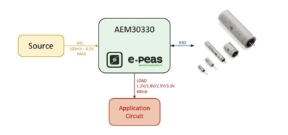
Figure 1 - E-Peas AEM30330 schematic (simplified)
For more information on the PMIC, please visit:
PB_AEM30330.pdf (e-peas.com)
AEM30330 product brief:
DS-AEM30330-v1.4.pdf (e-peas.com)
AEM30330 datasheet:
1.2. Why using LTO batteries from NICHICON?
Ultra-low harvesting charge with i.e. 0.01C (5µA) due to low internal resistance
Rapid charge/discharge with 20C
Increased charge/discharge cycles (up to 25.000 cycles)
Page 5
Very low self-discharge and operation at as low as -30⁰C
Extremely safe against rupture / ignition (UL1642 / IEC62133-2:2017)
Maintenance-free
0.35mAh (3.3x9mm L) up to 150mAh (12.5x40mm L)
For more information, please visit our dedicated site:
SLB series: Nichicon Small Lithium Titanate Rechargeable Batteries (nichiconbattery.com)
2. Product specification
Space for up to three parallel SLB batteries (no series connection available)
USBC charging with up to 20C / charge current can be set via switch
PMIC E-Peas AEM30330 with configuration jumpers (i.e. MPPT, load configuration etc.)
Harvesting source from either DC (i.e. indoor PV) or AC (i.e. piezo) available
11 measure and test point for evaluation purposes
DC and AC harvesting sources
PCBA size: 110 x 60mm
3. User Guide
The PCBA was initially designed as a harvester demonstration board including CO2 sensor (CozIR-Blink), a gas sensor
(Bosch BME688) and a Light sensor (LITE-ON LTR-329ALS) with data transmission via BLE /LoRa (Insight ISP4520). For
this evaluation board variant, these components have been removed from the PCBA so that individual harvesting
solutions can be designed.
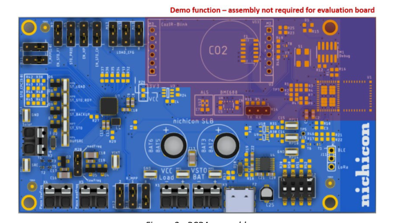
Figure 2 - PCBA assembly
Page 6
NOTE: The SLB batteries are not included, please contact NICHICON in order to obtain any of below battery ratings:
SLB03070LR35 2.4V / 0.35mAh, 12Ohm MAX 7mA max discharge current
SLB03090LR80 2.4V / 0.8mAh, 8Ohm MAX, 16mA max discharge current
SLB04255L040 2.4V / 4mAh, 0.6Ohm MAX, 80mA max discharge current
SLB08115L140 2.4V / 14mAh, 0.24Ohm MAX, 280mA max discharge current
SLB12400L151 2.4V / 150mAh, 0.06Ohm MAX, 3000mA max discharge current
3.1 Board features (connectors and jumpers)
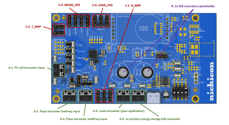
Figure 3 - Connectors and PMIC jumper settings
A. Five push-in connectors:
A-1. PV cell harvester input
A-2. Piezo harvester lowFreq input
A-3. Piezo harvester medFreq input
A-4. Load connector (your application)
A-5. Primary energy storage SLB connector
Note: the PCBA together with the PMIC is optimized to operate the energy storage device in the range of 1.8V
to 2.8V, hence please connect SLB series battery only for proper operation!
B. PCBA solder connection for energy storage
B-1. 2x SLB secondary placeholder
Each placeholder contains three lead pitch holes for different SLB battery ratings. The two placeholder pads
Page 7
are connected in parallel.
C. Four sets of 3-pin headers for PMIC adjustment:
C-1. Maximum power point ratio (R_MPP) configuration, for details refer to E-Peas charging IC
C-2. Maximum power point timing (T_MPP) configuration, for details refer to E-Peas charging IC
C-3. Load voltage configuration for VCC Load push-in terminal block. Please note that [3] has been removed from E-
Peas latest documentation and [1] and [0] are required:
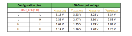
Table 1 - E-Peas load configuration (updated v.1.20 - removed LOAD_CFG[2])
C-4. PMIC mode configurations
Page 8
4. Getting started
Always connect the elements in the following order:
A. Reset the board: Short VINT, LOAD, STO and SRC test points to GND
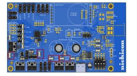
Figure 4 - Getting started
B. Configure the PCBA jumpers C-1 to C-4 according to your application requirements, see E-Peas AEM30330
datasheet as well as circuit diagram for PMIC in 9.1 for details on the jumper setting. These setting may contain:
- PMIC MPPT configuration (ratio / timing etc.)
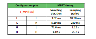
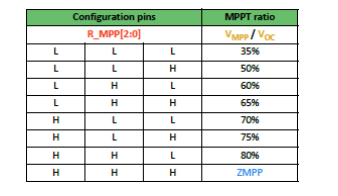
Table 2 - MPPT timing configuration
Table 3 - MPP ratio configuration
- Output load voltage configuration
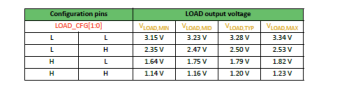
Table 4 - Load voltage configuration
- Mode configuration (EN_STO_FT; STO_PRIO; EN_HP; EN_STO_CH)
C. Connect the SLB storage element on VSTO_STO or on the SLB secondary placeholder (soldering required!)
D. Connect your application to A-4 load connector
Page 9
E. Connect the harvesting source (DC or AC) to either one of the SRC connectors:
A-1 for DC input (i.e. indoor PV cell)
A-2 for vibration harvester with lower frequency
A-3 for vibration harvester with medium frequency
NOTES:
To avoid damaging the board, users are required to follow this procedure!
Please select M28 jumper according to the frequency range (lowFreq / medFreq).
Please note E-Peas documentation are to be changed/modified after releasing this documentation. This
may affect the need to adjust the PMIC setting for an appropriate operation. Therefore, please always refer
to the latest E-Peas AEM30330 documentation!
Page 10
5. PCBA measure points
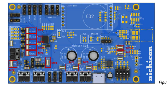
Figure 5 - PCBA Measure points
Please refer to below table for description on each measure point:
| No. | Signal Name | Function: |
| MP1 | VCC_Load | E-Peas harvesting IC output voltage. Supply for Sensors, MCU etc for your individual application. Output voltage 1.2V to 3.3V. |
| MP2 | SRC | +DC energy harvesting input, max 4.5V, 100mA |
| MP3 | VINT | Internal voltage supply, 2.2V |
| MP4 | BUFSRC | Connection to an external capacitor buffering the DCDC converter input. |
| MP5 | VSTO_BAT | Measure point for connected energy storage on Nichicon SLB battery voltage. |
| MP6 | ST_LOAD | Logic output. Asserted when VCC_Load rises above the typical load voltage VLOAD,TYP threshold. Reset when VCC_Load drops below V threshold. High level is VCC_Load. LOAD,MIN |
| MP7 | ST_STO | Logic output. Asserted when the storage device voltage rises above the V threshold. CHRDY Reset when the storage device voltage drops below VOVDIS threshold. High level is VSTO. |
| MP8 | ST_BACKUP | Logic output. Asserted when the storage element voltage VSTO drops below V OVDIS. High level is V . LOAD |
| MP9 | ST_STO_RDY | Logic output. Asserted when the storage element is above V . High level is V . CHRDY LOAD |
| MP10 | I_CHRG | Current Sense Amplifier Output for charge current. |
| MP11 | I_DISCHRG | Current Sense Output Amplifier for discharge current. |
Table 5 - Test and measure points
Page 11
6. SLB charging via USBC interface:
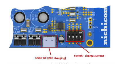
Figure 6 - USBC fast charge I/F
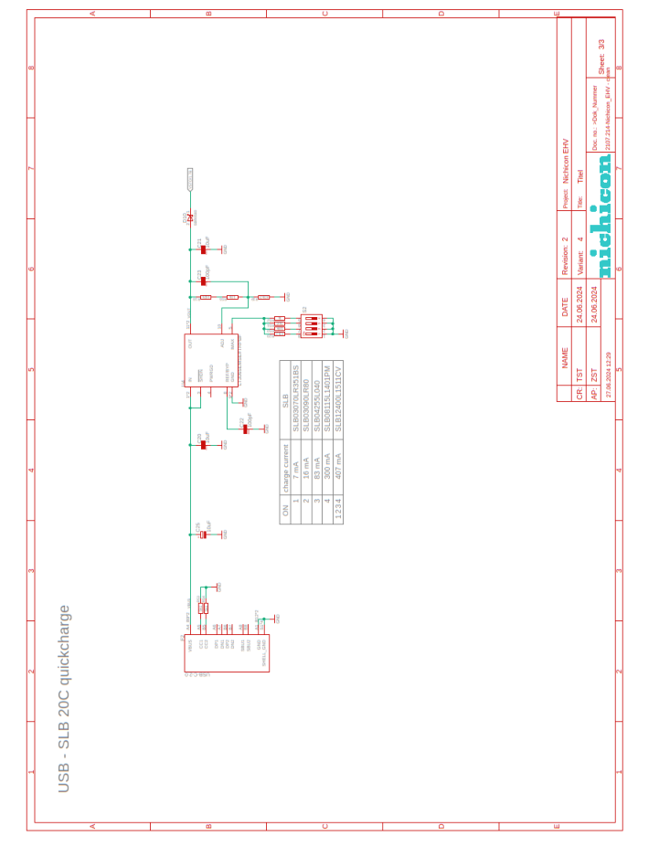
The PCBA features external USBC charging of the SLB battery with charging current up to 20C for quick validation.
Please select the correct charge current via the switches as shown in Table 6 below, which is also printed onto the
PCBA backside. Please note that the charge current reduces with the number of assembled SLB batteries.
Please always make sure not to apply charging current beyond 20C for proper board usage!
| SLB PN | SLB ratings | case size | switch setting | charge current | |||
| [-] | [-] | [mm] | 1 | 2 | 3 | 4 | [mA] |
| SLB03070LR35* | 3x7 (0.35mAh) | 3x7L | ON | OFF | OFF | OFF | 7 |
| SLB03090LR80* | 3.3x9 (0.8mAh) | 3.3x9L | OFF | ON | OFF | OFF | 16 |
| SLB04255L040* | 4x25.5 (4mAh) | 4x25.5L | OFF | OFF | ON | OFF | 80 |
| SLB08115L140* | 8x11.5 (14mAh) | 8x11.5L | OFF | OFF | OFF | ON | 280 |
| SLB12400L151* | 12.5x40 (150mAh) | 12.5x40L | ON | ON | ON | ON | 380 |
\*please note this is a generic part number and 3-digits will be added based on the lead wire configuration
Table 6 - SLB quick charging switch settings
Page 12
7. Appearance and PCBA interfaces
7.1. Appearance front
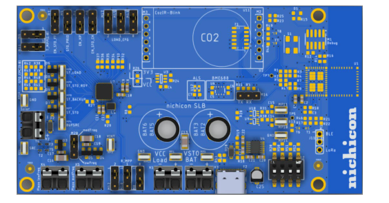
Figure 7 - PCBA front picture
7.2. Appearance back
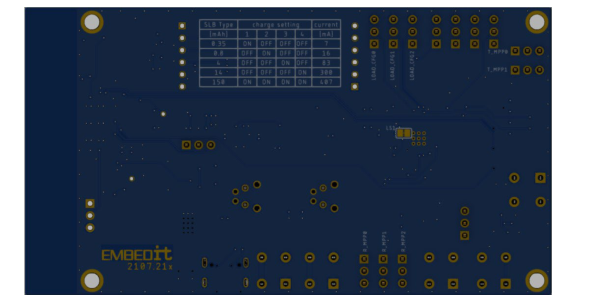
Figure 8 - PCBA rear picture
Page 13
8. Precaution for use
- Please use energy harvesting source according to the PMIC variant. Please also do not use both harvesting input
sources (PV and Piezo) at the same time!
- Do not short-circuit the secondary battery output. There is a risk of reduce in performance or component damage.
- Nichicon SLB batteries are polarized. Using with wrong polarity may cause reduce in performance or component
damage. Please connect Nichicon SLB battery with correct polarity onto the PCBA.
- Running the PMIC without C13 (100mF) minimum capacitance on STO or the SLB battery will permanently damage
the circuit.
9. SLB performance charts
9.1. Charge/discharge characteristics (SLB03070LR35\*)
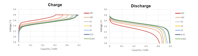
Figure 9- SLB charge/discharge characteristics (SLB03070LR35\*)
9.2. Self-discharge characteristics & SoC OCV plot(SLB03090LR80\*)
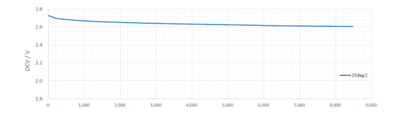
Figure 10 - self-discharge (SLB03090LR80\*)
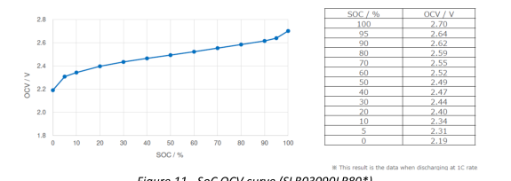
Figure 11 - SoC OCV curve (SLB03090LR80\*)
Page 14
10. Default PMIC settings
- PMIC priority setting has been set as default to LOAD.
- Custom storage element configuration for Nichicon SLB battery is set as below via resistors:
V_OVDIS: 1,80V
V_CHRDY: 2,40V
V_OVCH: 2,77V
- MPPT default configuration setting:
| Configuration pins | MPPT ratio | |||
| R_MPP[2] | R_MPP[1] | R_MPP[0] | VMPP / VOC | |
| AEM30330 | 1 | 1 | 0 | 85% |
Note: Please make sure to adjust configuration based on the optimum MPPT ratio of the used harvesting device!
11. Nichicon Ecosystem partners
Please visit Ecosystem Partners - Nichicon Small Lithium Titanate Rechargeable Batteries (nichiconbattery.com)
for ecosystem partners to explore available demos, distribution partners, manufacturers for PV cell, PMIC’s as well
as battery validation devices etc.
Page 15
12. Circuit diagram
12.1.
Power Management IC (PMIC) block
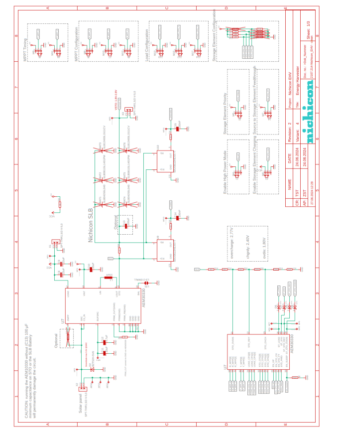
Figure 12 - PMIC schematic
Page 16
12.2.
AC-Source block
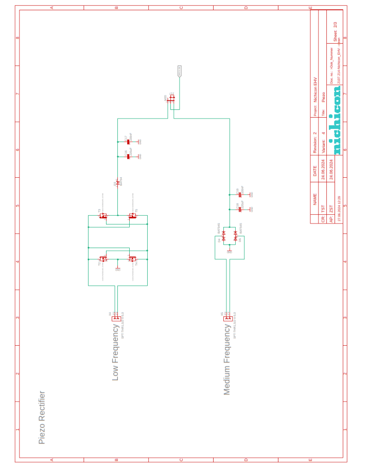
Figure 13 - Harvesting input
Page 17
Page 18
| Ref.No. | Description | Value | Manufacturer | Q't y | SchematicID |
|---|---|---|---|---|---|
| BT- 100016 | Chip-Resistor 1k 1% 0603 | 1k | 1 | R52 | |
| BT- 100022 | Chip-Resistor 0R 1% 0603 | 0 | 2 | R26, R29 | |
| BT- 100026 | Chip-Resistor 4k7 1% 0603 | 4.7k | 3 | R38, R39, R40 | |
| BT- 100027 | Chip-Resistor 10k 1% 0603 | 10k | 1 | R55 | |
| BT- 100053 | Kerko 100nF 50V 10% X7R 0603 | 100nF | 4 | C14, C15, C17, C19 | |
| BT- 100077 | Jumper RM2,54 Standard | Jumper RM2,54 Standard | 14 | J1, J2, J3, J4, J5, J6, J7, J8, J9, J10, J11, J12, J14, J17 | |
| BT- 100405 | Chip-Resistor 18k 1% 0603 | 18k | 1 | R50 | |
| BT- 100537 | Schottkydiode 30V/0.2A 5ns (BAT54) SOT23 | BAT54 | Diodes Inc. | 5 | D3, D6, D7, D8, D9 |
| BT- 100539 | Chip-Resistor 3.6k 1% 0603 | 3.6k | 1 | R51 | |
| BT- 100561 | Z-Diode 5.6V 0.4W 5% SOD- 123 (BZT52H) | BZT52H-5V6 | Nexperia | 1 | D2 |
| BT- 100689 | Dual Schottky Diode 30V, 0.2A | BAT54A | OnSemi | 2 | D4, D5 |
| BT- 100775 | Kerko 100pF, 50V, NP0, 5% 0603 | 100pF | 2 | C22, C23 | |
| BT- 100892 | Kerko 100uF 6.3V, 20% X5R, 1206 | 100uF | 1 | C13 | |
| BT- 100897 | Chip-Resistor 105k 1% 0603 | 105k | 1 | R8 | |
| BT- 101017 | Stiftleiste 1x3-position stehend, RM2.54mm, THR | STL-3-254-V-THR | 13 | M4, M5, M6, M7, M8, M9, M10, M11, M12, M13, M15, M17, M20 | |
| BT- 101057 | Chip-Resistor 5k1 1% 0603 | 5.1k | 2 | R53, R54 | |
| BT- 101082 | Phoenix Contact SPT - THR 1,5/ 2-V-5,0 P26 - vertical terminal block, 5mm pitch, 2-pin | SPT-THR1,5/2-V- 5,0 | 5 | X1, X2, X3, X4, X5 | |
| BT- 101086 | Kerko 220uF 6.3V 20% X5R 1206 | 220uF | 2 | C16, C18 | |
| BT- 101131 | Chip-Resistor 10M 1% 0603 | 10M | 2 | R33, R34 | |
| BT- 101213 | Schottkydiode 60V/0.5A SBR0560 SOD123 SMD | SBR0560 | 1 | D10 | |
| BT- 101299 | Kerko 10uF 35V 20% X5R 0603 | 10uF | 4 | C10, C11, C20, C21 | |
| BT- 101301 | Chip-Resistor 43k2 1% 0603 | 43.2k | 2 | R19, R20 | |
| BT- 101304 | Kerko 4.7uF 35V 20% X5R 0603 | 4.7uF | 1 | C12 |
Page 19
| BT- 101312 | Chip-Resistor 162k 1% 0603 | 162k | 2 | R18, R46 | |
| BT- 101449 | Kerko 22uF 10V X5R 0603 | 22uF | 2 | C8, C9 | |
| BT- 101464 | AEM30330 Ambient Energy Manager from e-peas | AEM30330 | e-Peas | 1 | U7 |
| BT- 101469 | Drossel 10uH 600mOhm, 0.9A, 2520 SMD | 10uH | Murata | 1 | L1 |
| BT- 101470 | MAX9610 1µA, µDFN/SC70, Lithium-Ion Battery, Precision Current-Sense Amplifier | MAX9610HEXK+T | Analog Devices | 2 | U9, U10 |
| BT- 101471 | N-Channel MOSFET 20V 0.6A 470mE RDSon PMZ600UNEL SOT883 | N-MOS- PMZ600UNEL- SOT883 | NXP | 2 | T2, T4 |
| BT- 101472 | P-Channel MOSFET -20V - 0.5A 1.4E RDSon PMZB950UPEL SOT883 | P-MOS- PMZB950UPEL- SOT883 | NXP | 2 | T3, T5 |
| BT- 101473 | Chip-Resistor 2.4R 1% 0603 | 2,4 | 3 | R30, R31, R45 | |
| BT- 101482 | Testpoint 5019 SMD | TESTPOINT-TP5019 | Keystone | 14 | MP1, MP2, MP3, MP4, MP5, MP6, MP7, MP8, MP9, MP10, MP11, MP12, MP13, MP14 |
| BT- 101487 | Chip-Resistor 22M 5% 0603 | 22M | 2 | R32, R37 | |
| BT- 101488 | Chip-Resistor 4.02M 1% 0603 | 4.02M | 2 | R35, R36 | |
| BT- 101495 | USB-Buchse Typ-C USB 2.0 Connector 24 (16+8 Dummy) | USB-C-2.0 | 1 | F2 | |
| BT- 101507 | DIP-switch with raised actuators, 2.54mm pitch, 4- positions, SMD | 1 | S2 | ||
| BT- 101508 | LT3065 500mA 45V LDO Programmable Current Limit 12MSOP | LT3065EMSE#TRPB F | LT | 1 | U4 |
| BT- 101515 | Elko 10uF/35V SMD 4x5.4mm | 10uF | 1 | C25 | |
| BT- 101524 | Chip-Resistor 1R 1% 0603 | 1 | 1 | R28 |
Page 20
Revision history
| Revision No. | Date | Content |
| 1.00 | 2024/06/20 | Initial release |
| 1.01 | 2024/06/27 | Fixed typos and spelling |
| 1.02 | 2024/06/28 | Include ecosystem partners on www.nichiconbattery.com |
| 1.03 | ||
| 1.04 | ||
| 1.05 |
Table 7 - Revision History
NICHICON (AUSTRIA) GmbH
Businesspark Marximum
Modecenterstrasse 17, Unit 2-7-A
1110 WIEN, AUSTRIA
+43 1 706 79 32
EMBED-IT GmbH
Kriehubergasse 16/1
1050 WIEN, AUSTRIA
office@embed-it.com
+43 1 336 00 66
Note: This board has been developed to help accelerating time to market for new harvesting devices with the use of
Nichicon SLB series. Therefore, the board is not intended to be used for commercial products etc.
IMPORTANT NOTICE – PLEASE READ CAREFULLY
NICHICON Corporation and its subsidiaries (“ST”) reserve the right to make changes, corrections, enhancements, modifications, and
improvements to Nichicon products and/or to this document at any time without notice. Purchasers should obtain the latest relevant
information on Nichicon products before placing orders. Nichicon products are sold pursuant to Nichicon’s terms and conditions of
sale in place at the time of order acknowledgement. Purchasers are solely responsible for the choice, selection, and use of Nichicon
products and Nichicon assumes no liability for application assistance or the design of Purchasers’ products. No license, express or
implied, to any intellectual property right is granted by Nichicon herein. Resale of Nichicon products with provisions different from
the information set forth herein shall void any warranty granted by Nichicon for such product. Nichicon and the Nichicon logo are
trademarks of Nichicon. All other product or service names are the property of their respective owners. Information in this document
Page 21
supersedes and replaces information previously supplied in any prior versions of this document.
© 2024 Nichicon Corporation – All rights reserved