Download PDF
SKI06106 ISC
Document overview
- PDF pages: 2
Technical content
Page 1
isc N-Channel MOSFET Transistor
SKI06106
FEATURES
- Drain Current –ID= 57A@ TC=25℃
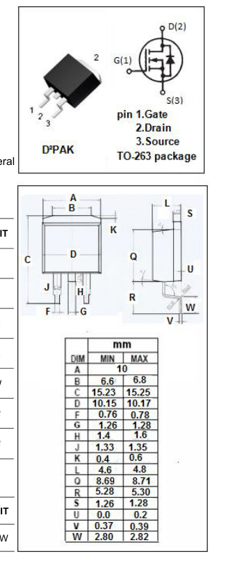
- Drain Source Voltage-
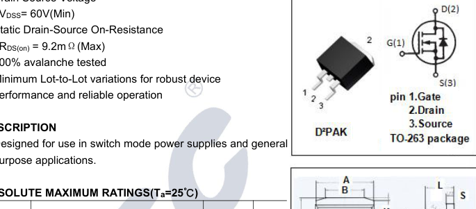
| SYMBOL | PARAMETER | VALUE | UNIT |
|---|---|---|---|
| V DSS | Drain-Source Voltage | 60 | V |
| V GS | Gate-Source Voltage-Continuous | ±20 | V |
| I D | Drain Current-Continuous | 57 | A |
| I DM | Drain Current-Single Pluse | 114 | A |
| P D | Total Dissipation @T =25℃ C | 90 | W |
| TJ | Max. Operating Junction Temperature | 150 | ℃ |
| Tstg | Storage Temperature | -55~150 | ℃ |
THERMAL CHARACTERISTICS
| SYMBOL | PARAMETER | MAX | UNIT |
|---|---|---|---|
| Rth j-c | Thermal Resistance, Junction to Case | 1.4 | ℃/W |
isc website:www.iscsemi.com
isc & iscsemi is registered trademark
Page 2
isc N-Channel MOSFET Transistor
SKI06106
ELECTRICAL CHARACTERISTICS
TC=25℃ unless otherwise specified
| SYMBOL | PARAMETER | CONDITIONS | MIN | MAX | UNIT |
|---|---|---|---|---|---|
| V (BR)DSS | Drain-Source Breakdown Voltage | V = 0; I = 0.1mA GS D | 60 | V | |
| V GS(th) | Gate Threshold Voltage | V = V ; I = 0.65mA DS GS D | 1.0 | 2.5 | V |
| R DS(on) | Drain-Source On-Resistance | V = 10V; I = 28.5A GS D | 9.2 | mΩ | |
| I GSS | Gate-Body Leakage Current | V = ±20V;V = 0 GS DS | ±100 | nA | |
| I DSS | Zero Gate Voltage Drain Current | V = 60V; V = 0 DS GS | 100 | μA | |
| V SD | Forward On-Voltage | I = 28.5A; V = 0 S GS | 1.5 | V |