
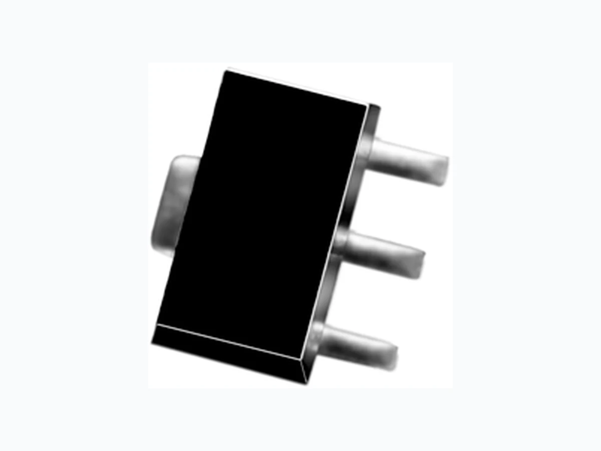
SHF-0289 ETC
Document overview
- Manufacturer or author: Provided By www.digicamel.com(FREE DATASHEET DOWNLOAD SITE)
- PDF pages: 8
Technical content
522 Almanor Ave., Sunnyvale, CA 94086 Phone: (800) SMI-MMIC http://www.stanfordmicro.com Preliminary EDS-101241 Rev A Product Description Preliminary SHF-0289 DC-3 GHz, 1.0 Watt GaAs HFET Product Features Patented GaAs Heterostructure FET Technology +30dBm Output Power at 1dB Compression +46dBm Output IP3 High Drain Efficiency: Up to 40% at Class AB 13 dB Gain at 900MHz (Application circuit) 13 dB Gain at 1900MHz (Application circuit)
Applications
Analog and Digital Wireless System Cellular PCS, CDPD, Wireless Data, Pagers Electrical Specifications at Ta = 25o C Stanford Microdevices SHF-0289 series is a high performance GaAs Heterostructure FET housed in a low-cost surface-mount plastic package. HFET technology improves breakdown voltage while minimizing Schottky leakage current for higher power added efficiency and improved linearity. Output power at 1dB compression for the SHF-0289 is +30dBm when biased for Class AB operation at 8V and 250mA. The +46 dBm third order intercept makes it ideal for high dynamic range, high intercept point requirements. They are well suited for use in both analog and digital wireless communication infrastructure and subscriber equipment including cellular PCS, CDPD, wireless data, and pagers. Adequate heat sinking must be provided for this part to avoid exceeding the maximum junction temperature. Methods include the use of screws near the device, and filled vias beneath the part to the ground plane. Refer to Mounting and Thermal Considerations section on page 7 for more information. The information provided herein is believed to be reliable at press time. Stanford Microdevices assumes no responsibility for inaccuracies or omissions. Stanford Microdevices assumes no responsibility for the use of this information, and all such information shall be entirely at the users own risk. Prices and specifications are subject to change without notice. No patent rights or licenses to any of the circuits described herein are implied or granted to any third party . Stanford Microdevices does not authorize or warrant any Stanford Microdevices product for use in life-support devices and/or systems. Copyright 2000 Stanford Microdevices, Inc. All worldwide rights reserved. Frequency (GHz) GMax(dB) Maximum Available Gain vs Frequency Vds = 8V, Idq = 250mA lobmyS snoitidnoCtseT:sretemaraP stinU .niM .pyT .xaM S| 12 |2 niaGrewoPnoitresnI Z,Am052=qdI,V0.8=sdV S Z= L smhO05= zHG9.0=f zHG9.1=f Bd 7.71 5.21 G xam niaGelbaliavAmumixaM Z,Am052=qdI,V0.8=sdV S Z= TPOS Z, L Z= TPOL zHG9.0=f zHG9.1=f Bd 32 PIOT tnioPtpecretnIredrOdrihTtuptuO )tuptuorewopmumixamrofdenutsieciveD( zHG9.0=f zHG9.1=f mBd mBd I ssD tnerruCniarDdetarutaS V0=sgV,V0.3=sdV Am0 56 Gm :ecnatcudnocnarT V0=sgV,V0.3=sdV Sm5 73 pV :egatloVffO-hcniP V sgb Am4.2=sgI,egatloVnwodkaerBecruoS-ot-etaG V2 2-7 1- V dgb Am4.2=dgI,egatloVnwodkaerBniarD-ot-etaG V2 2-7 1- htRd ael-ot-noitcnuj,ecnatsiseRlamrehT o W/C7 3
522 Almanor Ave., Sunnyvale, CA 94086 Phone: (800) SMI-MMIC http://www.stanfordmicro.com Preliminary EDS-101241 Rev A SHF-0289 DC-3GHz, 1 Watt GaAs HFET Preliminary Absolute Maximum Ratings Notes: 1. Operation of this device above any one of these parameters may cause permanent damage. retemaraPl obmyS etulosbA mumixaM egatloVecruoS-ot-niarDV SD V21+ egatloVecruoS-ot-etaGV SG V0otV5- erutarepmeTgnitarepOT PO C°58+otC54- rewoPtupnIFRP NI Wm002 erutarepmeTlennahCT HC C°571+ erutarepmeTegarotST GTS C°571+ot56- NOTE: I/V curves were taken using pulse sampling techniques. This results in low duty cycle currents through the device and therefore very low power levels. It is not recommended that these measurements be taken in d.c. mode, as excessive current could result in damage to the device. Plot of ID vs. VDS for VGS= -2.2V to 0V VDS (Volts) ID(amps) 0.1 0.2 0.3 0.4 0.5 0.6 0.7 012345678 VGS = 0 V VGS = - 0.2 V VGS = - 0.4 V VGS = - 0.6 V VGS = - 0.8 V VGS = - 1.0 V VGS = - 1.2 V VGS = -1.4 V VGS = -1.6 V VGS = -1.8 V VGS = -2.0 V VGS = -2.2 V
522 Almanor Ave., Sunnyvale, CA 94086 Phone: (800) SMI-MMIC http://www.stanfordmicro.com Preliminary EDS-101241 Rev A SHF-0289 DC-3GHz, 1 Watt GaAs HFET Preliminary |S21| & |S12| vs. Frequency GHz dB 012345 -40 -37 -34 -31 -28 -25 S21 S12 Typical s-parameters at 25°°°°° C (Vds = 8V, Idq = 250mA) zHGqerF S| 11 | S 11 gnA S 12 Bd S| 12 | S 12 gnA S 21 Bd S| 21 | S 21 gnA S| 22 | S 22 gnA S11 & S22 vs. Frequency (.05 to 4.5 GHz) Frequency (GHz) S21 (dB) S (dB) No external matching, scattering parameters de-embedded on test fixture to device lead at package edge.
522 Almanor Ave., Sunnyvale, CA 94086 Phone: (800) SMI-MMIC http://www.stanfordmicro.com Preliminary EDS-101241 Rev A SHF-0289 DC-3GHz, 1 Watt GaAs HFET Preliminary -30 -25 -20 -15 -10 -38 -35 -32 -29 -26 Frequency GHz Note: s-parameters determined using applications circuit shown above Frequency GHz S11 S22 S12 S21 0 5 10 15 20 Test Data @ 0.9 GHz P1dB(dBm) IP3(dBm) Output tone Level (dBm) 30.5 46.0 15 .gised.feRe ulaVe lytS/rebmuNtraP 7,1dCF p022s eires81HCMMHOR 21,8,6,2dCF p81s eires81HCMMHOR 01,3dCF p0001s eires81HCMMHOR 9,4dCF p001s eires81HCMMHOR 11,5dCF u1.0t lov53,"A"ezis,MULATNAT 1MCF p3.3s eires81HCMMHOR 2MCF p9.3s eires81HCMMHOR 1MLH n6.5K 6N5HF-8061LLOKOT 2MLH n7.4K 7N4HF-8061LLOKOT 1saibLH n93T N93HF-8061LLOKOT 2saibLH n28T N28HF-8061LLOKOT 2,1batsRs mho023 060ezis .gised.feRe ulaV 1Zz HM009@.ged0.6,smho05 2Zz HM009@.ged7.2,smho05 3Zz HM009@.ged5.8,smho05 4Zz HM009@.ged8.3,smho05 5Zz HM009@.ged4.3,smho05 6Zz HM009@.ged2.2,smho05 7Zz HM009@.ged0.6,smho05 8Zz HM009@.ged7.2,smho05 ς Ω 15 20 25 30 35 270 350 430 510 Drai n Effi ci ency ID
900 MHz Application Circuit at 25°°°°° C (Vds=8V, Idq=250mA)
Phase shift functional block between compo- nents are calculated based on wavelength of 900 MHz signal on FR4 board material with dielec- tric constant of 4.1, microstrip width and height dimensions of W=.054 inch and h= .031 inch. Microstrip Segment Specifications Pout (dBm) Pout vs. Pin T=25°°°°°C Drain Efficiency & I D vs. Pout T=25°°°°°C Efficiency (%) Pin (dBm) ID (mA) S11, S22 (dB) S21 (dB) S12 (dB) S11 & S22 vs. Frequency T=25°°°°°CS 21& S12vs. Frequency T=25°°°°°C Pout (dBm)
522 Almanor Ave., Sunnyvale, CA 94086 Phone: (800) SMI-MMIC http://www.stanfordmicro.com Preliminary EDS-101241 Rev A SHF-0289 DC-3GHz, 1 Watt GaAs HFET Preliminary -38 -35 -32 -29 -26 -30 -25 -20 -15 -10 Frequency GHz Frequency GHz S11 S12 S21 0 5 10 15 2 0 Pin (dBm) Note: s-parameters determined using applications circuit shown above Test Data @ 1.9 GHz P1dB(dBm) IP3(dBm) Output tone Level (dBm) 30.5 46.0 15 .gised.feRe ulaVe lytS/rebmuNtraP 1dCF p022s eires81HCMMHOR 8,7,6,3,2dCF p33s eires81HCMMHOR 9dCF p0001s eires81HCMMHOR 4dCF p001s eires81HCMMHOR 01dCF u1.0t lov53,"A"ezis,MULATNAT 5dCF u01t lov53,"A"ezis,MULATNAT 1MCF p7.2s eires81HCMMHOR 2MCF p2.2s eires81HCMMHOR 1saibLH n01T N01HF-8061LLOKOT 2saibLH n22T N22HF-8061LLOKOT 1batsRs mho1.53 060ezis 2batsRs mho023 060ezis .gised.feRe ulaV 1Zz HM0091@.ged5.5,smho05 2Zz HM0091@.ged9.71,smho05 3Zz HM0091@.ged5.5,smho05 4Zz HM0091@.ged72,smho05 5Zz HM0091@.ged8.5,smho05 ς Ω S22 15 20 25 30 35 27 0 35 0 43 0 51 0 Drai n Eff i ci ency ID Pout(dBm) Phase shift functional block between components are calculated based on wavelength of 1900 MHz signal on FR4 board material with dielectric con- stant of 4.1, microstrip width and height dimen- sions of W=.054 inch and h= .031 inch. Pout vs. Pin T=25οC Pout (dBm)S11, S22 (dB) S11 & S22 vs. Frequency T=25oC S21 & S12 vs. Frequency T=25oC Efficiency (%) Drain Efficiency & IDvs. Pout T=25οC S21 (dB) ID (mA)S12 (dB)
1.9 GHz Application Circuit at 25°°°°° C (Vds=8V, Idq=250mA)
Microstrip Segment Specifications
522 Almanor Ave., Sunnyvale, CA 94086 Phone: (800) SMI-MMIC http://www.stanfordmicro.com Preliminary EDS-101241 Rev A SHF-0289 DC-3GHz, 1 Watt GaAs HFET Preliminary -30 -25 -20 -15 -10 Pin (dBm) Frequency GHz Frequency GHz S12 S21 S11 S22 0 5 10 15 20 25 Note: s-parameters determined using applications circuit shown above Test Data @ 2.45 GHz P1dB(dBm) IP3(dBm) Output tone Level (dBm) 31.0 44.5 15 -38 -35 -32 -29 -26 .gised.feRe ulaVe lytS/rebmuNtraP 5,2dCF p6.5s eires81HCMMHOR 8,7,6,3,1dCF p22s eires81HCMMHOR 9dCF p0001s eires81HCMMHOR 4dCF p001s eires81HCMMHOR 01dCF u1.0t lov53,"A"ezis,MULATNAT 1MCF p5.1s eires81HCMMHOR 2MCF p2.1s eires81HCMMHOR 1saibLH n51T N51HF-8061LLOKOT 2saibLH n51T N51HF-8061LLOKOT 1batsRs mho1.53 060ezis 2batsRs mho013 060ezis .gised.feRe ulaV 1Zz HM0542@.ged3.7,smho05 2Zz HM0542@.ged7.21,smho05 3Zz HM0542@.ged3.01,smho05 4Zz HM0542@.ged3.01,smho05 5Zz HM0542@.ged8.51,smho05 6Zz HM0542@.ged9.81,smho05 7Zz HM0542@.ged1.7,smho05 ς Ω 10 15 20 25 30 35 270 350 430 510 Drai n Effi ci ency ID Drain Efficiency & ID vs. Pout T=25oCPout vs. Pin T=25oC Microstrip Segment Specifications Efficiency (%)S21 (dB) S11 & S22 vs. Frequency T=25oC S12 (dB) I D (mA) S11 & S22 vs. Frequency T=25oC Pout (dBm)S11, S22 (dB) Pout (dBm) Phase shift functional block between components are calculated based on wavelength of 2450 MHz signal on FR4 board material with dielectric constant of 4.1, microstrip width and height dimensions of W=.054 inch and h= .031 inch.
2.45 GHz Application Circuit at 25°°°°° C (Vds=8V, Idq=250mA)
522 Almanor Ave., Sunnyvale, CA 94086 Phone: (800) SMI-MMIC http://www.stanfordmicro.com Preliminary EDS-101241 Rev A SHF-0289 DC-3GHz, 1 Watt GaAs HFET Preliminary rebmuNtraP rePseciveD leeR eziSleeR 9820-FHS0 001" 7 Part Number Ordering Information Mounting and Thermal Considerations: It is very important that adequate heat sinking be provided to avoid exceeding the maximum device junction temperature. All of the following suggestions should be followed to ensure maximum operating life of the device: 1. Use 2 ounce copper if possible. 2. Use a large ground pad area with many plated through- holes (solder filling is recommended). 3. Multiple filled vias are required directly below the SOT- 89 ground tab. 4. Solder the copper pad on the backside of the device package to the ground plane. 5. Use three point board seating with 2-56 machine screws (no more than 0.2 inch from the device) to provide a low thermal resistance path to the plate. The thermal resistance from ground lead to screws is 2 deg. C/W 6. We recommend thermal transfer paste be used between the board and the mounting plate. Part Symbolization Outline Drawing Caution: ESD sensitive Appropriate precautions in handling, packaging and testing devices must be observed. niP noitangiseD 1e taG 2e cruoS 3n iarD 4e cruoS The part will be symbolized with a H2 designator on the top surface of the package.
522 Almanor Ave., Sunnyvale, CA 94086 Phone: (800) SMI-MMIC http://www.stanfordmicro.com Preliminary EDS-101241 Rev A SHF-0289 DC-3GHz, 1 Watt GaAs HFET Preliminary Component Tape and Reel Packaging Tape Dimensions noitpircseDl obmyS eziS )mm( leel ytivaCh tgneL htdiW htpeD hctiP retemaiDeloHmottoB A B K P 10.0-/+19.4 10.0-/+25.4 10.0-/+09.1 10.0-/+00.8 01.0-/+06.1 noitarofrePr etemaiD hctiP noitisoP E 50.0-/+55.1 10.0-/+00.4 10.0-/+57.1 epaTrevoCh tdiW ssenkcihTepaT C t 52.0-/+01.9 10.0-/+50.0 epaTreirraCh tdiW ssenkcihT W T 30.0-/+0.21 50.0-/+03.0 ecnatsiDn oitarofrePotytivaC )noitceriDhtdiW( noitarofrePotytivaC )noitceriDhtgneL( F 01.0-/+05.5 01.0-/+00.2 Note: Drawing not to scale For 89 Outline