
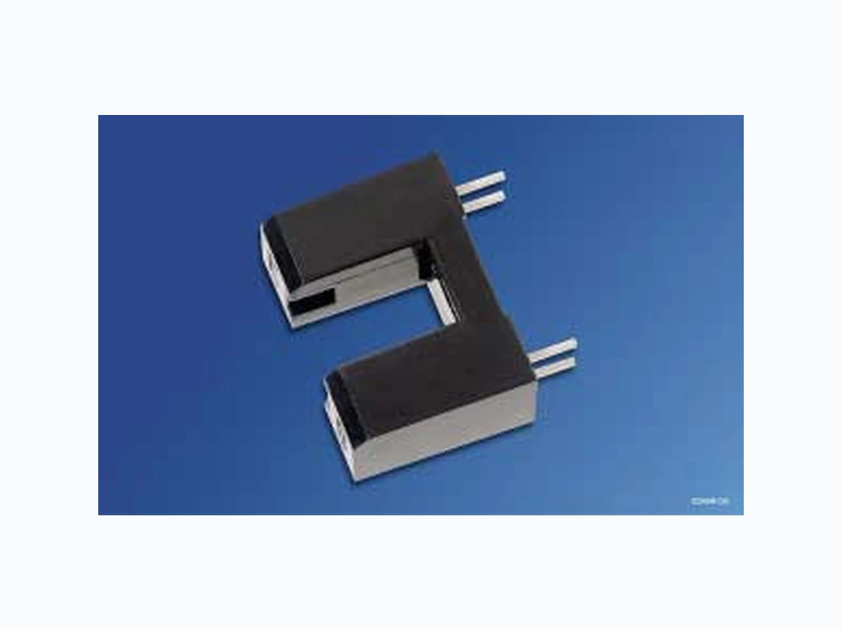
SFH9315 OSRAM
Document overview
- Manufacturer or author: Provided By www.digicamel.com(FREE DATASHEET DOWNLOAD SITE)
- PDF pages: 8
Technical content
Features
Compact type GaAs infrared emitter (950 nm) Silicon phototransistor detector with daylight-cutoff filter
Applications
Speed control Motor control Monitoring of paper feed in printers, copiers, facsimiles Disk drives Control of print head in printers Coin detection Optoelectronic switches
Grenzwerte TA = 25 °C Maximum Ratings Bezeichnung Parameter Symbol Symbol Wert Value Einheit Unit Sender (GaAs-Diode) Emitter (GaAs Diode) Sperrspannung Reverse voltage VR 5 V Durchlaßstrom Forward current IF (DC) 40 mA Verlustleistung Power dissipation Ptot 65 mW Wärmewiderstand Thermal resistance RthJA 280 K/W Empfänger (Si-Fototransistor) Detector (Silicon Phototransistor) Kollektor-Emitter-Spannung Collector-emitter voltage VCE 15 V Kollektor-Emitter-Spannung, (t ≤ 2 min) Collector-emitter voltage, (t ≤ 2 min) VCE 30 Emitter-Kollektor-Spannung Emitter-collector voltage VEC 7 Kollektorstrom Collector current IC 15 mA Verlustleistung Total power dissipation Ptot 65 mW Wärmewiderstand Thermal resistance RthJA 280 K/W Gabellichtschranke Slotted Interrupter Lagertemperatur Storage temperature range Tstg – 40 … + 85 °C Betriebstemperatur Operating temperature range Top – 40 … + 85 Elektrostatische Entladung Electrostatic discharge ESD 2 kV
Kennwerte TA = 25 °C Characteristics Bezeichnung Parameter Symbol Symbol Wert Value Einheit Unit Sender (GaAs-Diode) Emitter (GaAs Diode) Wellenlänge der Strahlung Wavelength of peak emission λpeak 950 nm Durchlaβspannung Forward voltage IF = 20 mA, tp = 20 ms VF 1.2 (≤ 1.4) V Sperrstrom Reverse current VR = 5 V IR 0.01 (≤ 1) μA Kapazität Capacitance VR = 0 V, f = 1 MHz C0 16 pF Empfänger (Si-Fototransistor) Detector (Silicon Phototransistor) Wellenlänge der max. Fotoempfindlichkeit Wavelength of max. sensitivity λS max 920 nm Spectr. Bereich der Fotoempfindlichkeit Spectral range of sensitivity S = 10% of Smax λ 840 … 1080 nm Kapazität Capacitance VCE = 0 V, f = 1 MHz, E = 0 CCE 4.5 pF Dunkelstrom Dark current VCE = 20 V ICEO 2 (≤ 50) nA
IF = 20 mA; VCE = 5 V ICE min. 0.7 mA Kollektor-Emitter-Sättigungsspannung Collector-emitter-saturation voltage IF = 20 mA; IC = 0.2 mA VCE sat ≤ 0.4 V Anstiegs- und Abfallzeit Rise and fall time VCC = 5 V, IC = 1 mA, RL = 1 kΩ tr tf μs μs Kennwerte TA = 25 °C Characteristics (cont’d) Bezeichnung Parameter Symbol Symbol Wert Value Einheit Unit
Forward Current IF = f (VF) Single pulse, tp = 20 μs 10-2 10-1 101 102
103 OHF00630
V mA 1 2 3 4 5 Max. Permissible Forward Current IF = f (TA) OHF00628 IF T mA A 20 40 60 80 ˚C 100 = 280 K/WRthJA Dark Current ICEO = f (TA) VCE = 20 V, E = 0 T OHF00380 A CEOΙ -110 10 0 10 1 10 2 10 3 nA 20 40 60 80 100˚C
Maßzeichnung Package Outlines Maße in mm (inch) / Dimensions in mm (inch). GPXY6010 Emitter Sensor 14.0 (0.551) 14.4 (0.567) 10.5 (0.413) 10.1 (0.398) 4.8 (0.189) 5.2 (0.205) 3.5 (0.138) 7.8 (0.307) Optical axis 5.8 (0.228) 6.2 (0.244) 2.74 (0.108) 2.34 (0.092) 8.0 (0.315) 10.5 (0.413) 10.1 (0.398) 2.0 (0.079) 0.5 (0.020) 0.3 (0.012) 7.7 (0.303) 2.5 (0.098) 0.4 (0.016) 0.6 (0.024) 0.6 (0.024) 0.4 (0.016) Circuitry Marking this side 2.54 (0.100)
Lötbedingungen Soldering Conditions Wellenlöten (TTW) (nach CECC 00802) TTW Soldering (acc. to CECC 00802) Löthinweise Soldering Conditions Bauform Type Tauch-, Schwalllötung Dip, Wave Soldering Reflowlötung Reflow Soldering Kolbenlötung Iron Soldering Peak Temp. (solderbath) Max. Time in Peak Zone Peak Temp. (package temp.) Max. Time in Peak Zone (Iron temp.) SFH 9315 260 °C 10 s n. a. – 300 °C < 5 s OHLY0598 50 100 150 200 250 100 150 200 250 300 T t C s 235 C 10 s C... 260 1. Welle 1. wave 2. Welle 2. wave
5 K/s 2 K/sca 200 K/s
CC... 130100
2 K/s
Zwangskühlung forced cooling Normalkurve standard curve Grenzkurven limit curves
Published by OSRAM Opto Semiconductors GmbH Wernerwerkstrasse 2, D-93049 Regensburg www.osram-os.com © All Rights Reserved. Attention please! The information describes the type of component and shall not be considered as assured characteristics. Terms of delivery and rights to change design reserv ed. Due to technical requirements components may contain dangerous substances. For information on the types in question please contact our Sales Organization. Packing Please use the recycling operators known to you. We can also help you – get in touch with your nearest sales office. By agreement we will take packing material back, if it is sorted. You must bear the costs of tr ansport. For packing material that is returned to us unsorted or which we are not obliged to accept, we shall have to invoice you for any costs incurred. Components used in life-support devices or system s must be expressly authorized for such purpose! Critical components 1 , may only be used in life-support devices or systems 2 with the express written approval of OSRAM OS. 1 A critical component is a component usedin a life-support device or system whose failure can reasonably be expected to cause the failure of that life-support device or system, or to affect its safety or effectiveness of that device or system. 2 Life support devices or systems are intended (a) to be implanted in the human body, or (b) to support and/or maintain and sustain human life. If they fail, it is reasonable to assume that the health of the user may be endangered.