
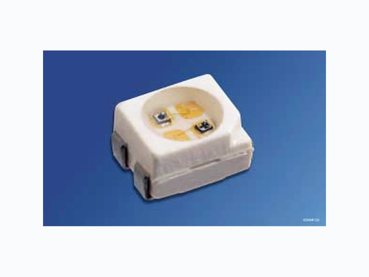
SFH7222 OSRAM
Document overview
- Manufacturer or author: Provided By www.digicamel.com(FREE DATASHEET DOWNLOAD SITE)
- PDF pages: 11
Technical content
Features
SMT package with IR emitter (880 nm) and green emitter (565 nm) Suitable for SMT assembly Available on tape and reel Emitter und detector can be controlled separately
Applications
Combination of display with: – data transmission – remote control – infrared interface
Die angegebenen Grenzdaten gelten für einen Chip, wenn nicht anders angegeben. The stated maximum ratings refer to one chip, unless otherwise specified. Grenzwerte Maximum Ratings Bezeichnung Parameter Symbol Symbol Wert Value Einheit Unit IRED LED Betriebstemperatur Operating temperature range Top – 40 … + 100 – 40 … + 100 °C Lagertemperatur Storage temperature range Tstg – 40 … + 100 – 40 … + 100 °C Sperrspannung Reverse voltage VR 5 5 V Durchlassstrom Forward current IF (DC) 100 30 mA Stoßstrom Surge current tp ≤ 10 μs, D = 0 IFSM 2.5 0.5 A Verlustleistung Total power dissipation Ptot 180 100 mW Wärmewiderstand Thermal resistance junction/ambient1) Rth JA 450 500 K/W Wärmewiderstand Thermal resistance junction/ambient2) Rth JA 650 K/W 1) nur ein Chip betrieben / only one chip on 2) beide Chips betrieben / both chips on
Kennwerte (TA = 25 °C) Characteristics Bezeichnung Parameter Symbol Symbol Wert Value Einheit Unit IRED LED Wellenlänge der Strahlung Wavelength of peak emission IF = 100 mA λpeak 880 565 (IF = 10 mA) nm Dominantwellenlänge Dominant wavelength IF = 10 mA λdom – 570 nm Spektrale Bandbreite bei 50% von Imax Spectral bandwidth at 50% of Imax IF = 100 mA Δλ 80 25 (IF = 10 mA) nm Abstrahlwinkel Half angle ϕ ± 60 ± 60 Grad deg. Abmessungen der aktiven Chipfläche Dimensions of the active chip area L × B L × W 0.4 × 0.4 0.25 × 0.25 mm2 Schaltzeiten Switching times 10%/90%, IF = 100 mA, RL = 50 Ω tr, tf 500 450, 200 ns Kapazität Capacitance VR = 0 V, f = 1 MHz Co 25 15 pF Durchlassspannung Forward voltage IF = 10 mA IF = 100 mA, tp = 20 ms IF = 1 A, tp = 100 μs VF 1.5 (≤ 1.8) 3.0 (≤ 3.8) 2.0 (≤ 2.6) V Sperrstrom, VR = 5 V Reverse current Gesamtstrahlungsfluss Total radiant flux IF = 100 mA, tp = 20 ms Φe 23 – mW Lichtstärke Luminous intensity IF = 2 mA IV – >0.25 mcd Temperaturkoeffizient von Ie bzw. Φe Temperature coefficient of Ie or Φe IF = 100 mA
IRED Radiation Characteristics Irel = f (ϕ) LED Directional Characteristics Srel = f (ϕ) Temperaturkoeffizient von VF Temperature coefficient of VF IF = 100 mA TCV – 2 – 1.4 mV/K Temperaturkoeffizient von λ Temperature coefficient of λ IF = 100 mA TCλ + 0.25 0.30 (λpeak) 0.07 (λdom) nm/K Strahlstärke Ie der IRED in Achsrichtung gemessen bei einem Raumwinkel Ω = 0.01 sr Radiant Intensity Ie of the IRED in Axial Direction at a solid angle of Ω = 0.01 sr Bezeichnung
Description
Strahlstärke Radiant intensity IF = 100 mA, tp = 20 ms Ie min. ≥ 4 mW/sr Strahlstärke Radiant intensity IF = 1 A, tp = 100 μs Ie typ. 48 mW/sr Kennwerte (TA = 25 °C) Characteristics (cont’d) Bezeichnung Parameter Symbol Symbol Wert Value Einheit Unit IRED LED 0.2 0.4 1.0 0.8 0.6 ϕ 1.0 0.8 0.6 0.4 50˚ 60˚ 70˚ 80˚ 90˚ 100˚
Forward Current IF = f (VF) TA = 25 °C Max. Permissible Forward Current IF = f (TA) OHR00881 FV -210 -110 010 110 01 2 3 4 5 6 V 8 AΙ F OHR00883 FΙ 100 120 20 40 60 80 100 120 mA TA RthjA = 450 K/W Rel Luminous Intensity IV / IV(10 mA) = f (IF) TA = 25 °C Relative Spectral Emission Irel = f (λ) OHR00878 Ι e FΙ -210 -110 010 110 210 010 10 1 10 2 10 4mA eΙ (100mA) 310 750 Ι rel OHR00877 800 850 900 950 nm 1000 100 λ Perm. Pulse Handling Capability IF = f (tp), Duty cycle D = parameter, TA = 25 °C Ι F OHR00886 210 310 410 mA -510 s FΙ T DC 0.005=D pt T t p pt 0.5 0.2 0.1 0.01 0.02 0.05 10-4 10-3 10-2 10-1 100 101 102
Forward Current IF = f (VF) TA = 25 °C Max. Permissible Forward Current IF = f (TA) Forward Voltage VF = f (TA) IF = f (TA) 10 -1 V green OHF00577 Ι F FV 010 110 210 mA 1 chip on2 chips on mA ˚C0 IF OHL00241 20 40 60 80 100 TA temp. ambient T green 1.4 OHF00581 VF AT 0 20 40 60 80 100 1.6 1.8 2.0 2.2 V 2.4 Relative Luminous Intensity IV / IV(10 mA) = f (IF), TA = 25 °C Wavelength at Peak Emission λpeak = f (TA), IF = 10 mA Relative Luminous Intensity IV / IV(25 °C) = f (IF), IF = 10 mA V V (10 mA) 10 -1 0 10 10 12 10mA green 10 -3 OHF00578 FΙ -210 -110 010 110 Ι Ι green 550 OHF00579 λpeak AT 0 20 40 60 80 100 570 590 610 630 650 nm 690 green 0.0 OHF00582 AT 0 20 40 60 80 100 V VΙ Ι 0.4 0.8 1.2 1.6 2.0 (25 ˚C) Perm. Pulse Handling Capability IF = f (tp) Duty cycle D = parameter, TA = 25 °C Dominant Wavelength λdom = f (TA), IF = 10 mA OHL01686 s10-5 10-4 10-3 10-2 10-1 100 101 t D I T T P F tP= D = 0.005 0.01 0.02 0.05 0.2 0.5 DC 10 1 IF t 210 0.1 p 10 3 mA green 550 OHF00580 λdom AT 0 20 40 60 80 100 570 590 610 630 650 nm 690
Maßzeichnung Package Outlines Maße in mm (inch) / Dimensions in mm (inch). Gehäuse / Package weiß, klarer Verguss / white, clear resin Anschlussbelegung pin configuration 1: Kathode (cathode) 880nm 2: Anode (anode) 880nm 3: Kathode (cathode) 565nm 4: Anode (anode) 565nm GEOY7023 0.7 (0.028) 0.9 (0.035) 1.7 (0.067) 2.1 (0.083) 0.12 (0.005) 0.18 (0.007) 0.5 (0.020) 3.7 (0.146) 0.4 (0.016) 0.6 (0.024) 2.6 (0.102) 3.0 (0.118) 2.1 (0.083) 2.3 (0.091) Package marking 3.0 (0.118) 3.4 (0.134) (2.4 (0.095)) 0.6 (0.024)
Empfohlenes Lötpaddesign Recommended Solder Pad Maße in mm (inch) / Dimensions in mm (inch). OHLPY439 Padgeometrie für verbesserte Wärmeableitung improved heat dissipation Paddesign for Lötstoplack Solder resist 1.1 (0.043) 4.5 (0.177) 1.5 (0.059) 2.6 (0.102) 3.3 (0.130) 0.5 (0.020) 7.5 (0.295) 0.4 (0.016) Cathode marking Kathoden Markierung / Cu Fläche / 12 mm per pad2 Cu-area 3.3 (0.130)
Lötbedingungen Vorbehandlung nach JEDEC Level 2 Soldering Conditions Preconditioning acc. to JEDEC Level 2 Reflow Lötprofil für bleifreies Löten (nach J-STD-020C) Reflow Soldering Profile for lead free soldering (acc. to J-STD-020C) Wellenlöten (TTW) (nach CECC 00802) TTW Soldering (acc. to CECC 00802) OHLA0687 T t s 120 s max 100 150 200 250 300 Ramp Up 100 s max 50 100 150 200 250 300 Ramp Down
6 K/s (max)
3 K/s (max)
25 ˚C 30 s max 260 ˚C+0 ˚C -5 ˚C 245 ˚C±5 ˚C 240 ˚C 255 ˚C 217 ˚C Maximum Solder Profile Recommended Solder Profile 235 ˚C-0 ˚C +5 ˚C Minimum Solder Profile 10 s min OHLY0598 50 100 150 200 250 100 150 200 250 300 T t C s 235 C 10 s C... 260 1. Welle 1. wave 2. Welle 2. wave
5 K/s 2 K/sca 200 K/s
CC... 130100
2 K/s
Zwangskühlung forced cooling Normalkurve standard curve Grenzkurven limit curves
OSRAM Opto Semiconductors GmbH Wernerwerkstrasse 2, D-93049 Regensburg www.osram-os.com © All Rights Reserved. The information describes the type of component and shall not be considered as assured characteristics. Terms of delivery and rights to change design reserv ed. Due to technical requirements components may contain dangerous substances. For information on the types in question please contact our Sales Organization. Packing Please use the recycling operators known to you. We can also help you – get in touch with your nearest sales office. By agreement we will take packing material back, if it is sorted. You must bear the costs of tr ansport. For packing material that is returned to us unsorted or which we are not obliged to accept, we shall have to invoice you for any costs incurred. Components used in life-support devices or system s must be expressly authorized for such purpose! Critical components 1 , may only be used in life-support devices or systems 2 with the express written approval of OSRAM OS. 1 A critical component is a component usedin a life-support device or system whose failure can reasonably be expected to cause the failure of that life-support device or system, or to affect its safety or effectiveness of that device or system. 2 Life support devices or systems are intended (a) to be implanted in the human body, or (b) to support and/or maintain and sustain human life. If they fail, it is reasonable to assume that the health of the user may be endangered.
720-SFH7222-Z - Osram Opto Semiconductor SFH 7222-Z