
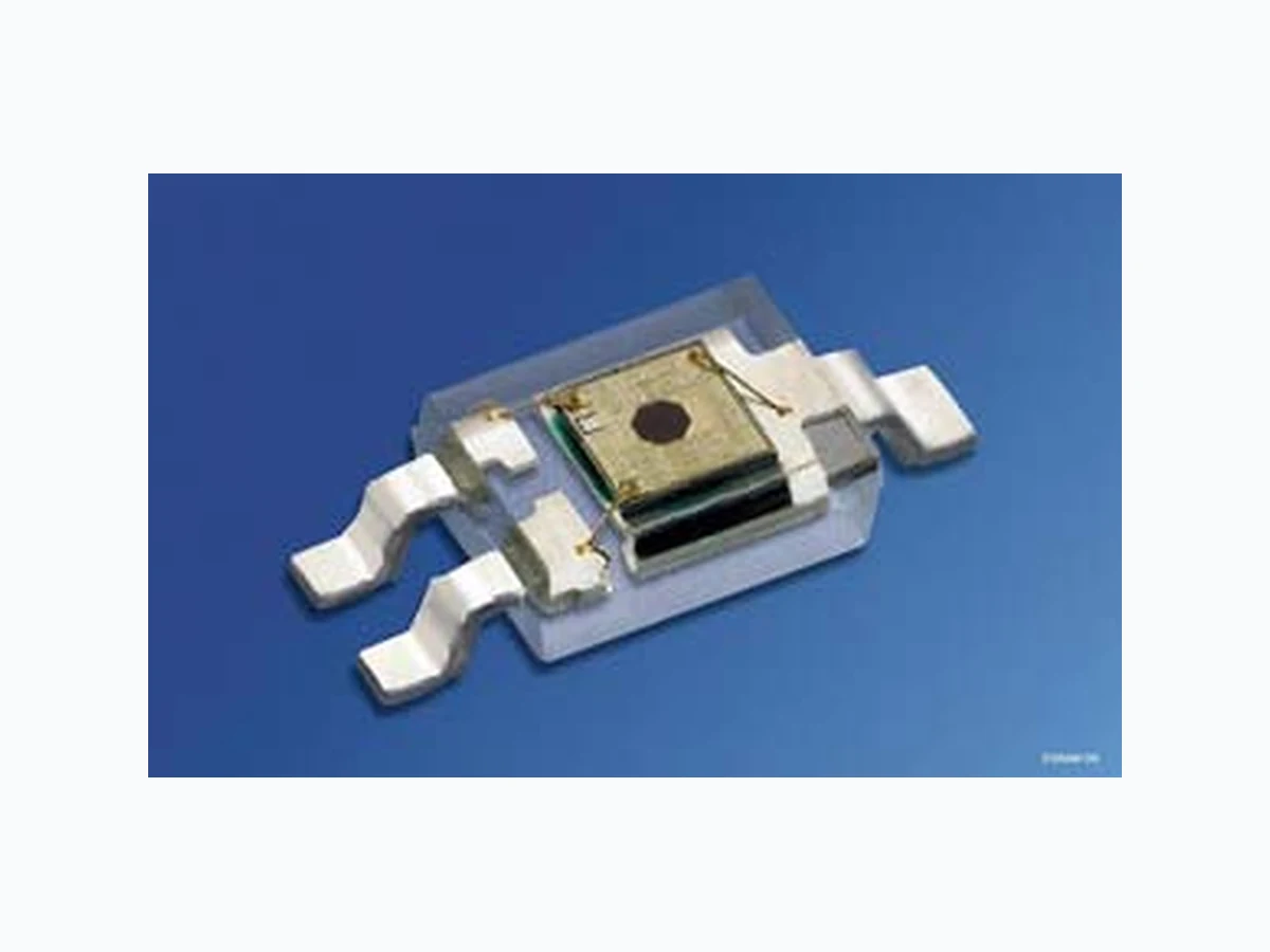
SFH5440_07 OSRAM
Document overview
- Manufacturer or author: Provided By www.digicamel.com(FREE DATASHEET DOWNLOAD SITE)
- PDF pages: 7
Technical content
Features
SFH 5440: Output active low SFH 5441: Output active high Available on tape and reel Suitable for applications from 400 nm to 1100 nm
Applications
Optical threshold switch P u l s e f o r m e r Counter
SFH 5440, SFH 5441 Zur Stabilisierung der Versorgung wird ein Stützkondensator (angeschlossen zwischen VCC und GND) von typ. 0.1 µF empfohlen. A bypass capacitor, 0.1 µF typical, connected between VCC and GND is recommended in order to stabilize power supply line. Grenzwerte (TA = 25 °C) Maximum Ratings Bezeichnung Parameter Symbol Symbol Wert Value Einheit Unit Lagertemperatur Storage temperature range Tstg – 40 … + 100 °C Betriebstemperatur Operating temperature range Top – 40 … + 85 °C Versorgungsspannung Supply voltage VCC – 0.5 … + 20 V Ausgangsspannung Output voltage VO – 0.5 … + 20 V Ausgangsstrom Output current IO 50 mA Verlustleistung Power dissipation Ptot 175 mW Empfohlener Arbeitsbereich Recommended Operating Conditions Bezeichnung Parameter Symbol Symbol Wert Value Einheit Unit Versorgungsspannung Supply voltage VCC 4 … 18 V Ausgangsstrom Output current IO < 16 mA Kennwerte (TA = 25 °C, VCC = 5 V) Characteristics Bezeichnung Parameter Symbol Symbol Wert Value Einheit Unit Ausgangsspannung „high“ Output voltage “high” IO = 0 VOH VCC (> 4.0) V Ausgangsspannung „low“ Output voltage “low” IO = 16 mA VOL 0.15 (< 0.4) V
SFH 5440, SFH 5441 2007-09-18 3 Stromaufnahme, E = 0 Supply current VCC = 5 V VCC = 18 V ICC 3.3 (< 5) 5.0 mA Schaltschwelle, λ = 950 nm Threshold “ON“ Ee, ON 170 (< 320) µW/cm2 Hysterese Hysteresis Ee, OFF/Ee, ON 0.6 (0.5 … 0.9) Halbwinkel Half angle ϕ± 60 Grad degr. Anstiegszeit 10% bis 90% Rise time 10% to 90% RL = 280 Ω, Ee = 600 µW/cm2, λ = 950 nm tr 100 ns Abfallzeit 90% bis 10% Fall time 90% to 10% RL = 280 Ω, Ee = 600 µW/cm2, λ = 950 nm tf 100 ns Ausgangsverzögerungszeit Propagation delay time “H” → “L” RL = 280 Ω, Ee = 600 µW/cm2, λ = 950 nm tPHL 5 (< 15) µs Ausgangsverzögerungszeit Propagation delay time “L” → “H” RL = 280 Ω, Ee = 600 µW/cm2, λ = 950 nm tPLH 5 (< 15) µs Kennwerte (TA = 25 °C, VCC = 5 V) Characteristics (cont’d) Bezeichnung Parameter Symbol Symbol Wert Value Einheit Unit
SFH 5440, SFH 5441 2007-09-18 5 Relative Threshold Ee, ON/Ee, ON (Vcc = 5 V) = f (VCC) Output Voltage VOL= f (IOUT, VCC) OHF00507 0.5 0 5 10 15 20 0.6 0.7 0.8 0.9 1.1 1.2 1.3 1.5 V E VCC e, ON Ee, ON_5 V OHF00512 0 01 0 20 30 40 50mA 5 V OUTI 0.5 1.5 2.5 3.5 OLV V 10 V 15 V 20 V Supply Current ICC = f (VCC) Supply Current vs. Ambient Temperature ICC = f (TA, VCC) OHF00510 0 0 5 10 15 20 V mA CCI VCC OHF00514 0-25 mA CCI AT 0 25 50 75 100˚C CCV = 5 V = 10 VCCV = 20 VVCC = 15 VVCC Total Power Dissipation Ptot = f (TA) OHF01322 0 0 totP AT 20 40 60 80 ˚C 100 100 120 140 160 200 mW
SFH 5440, SFH 5441 Maßzeichnung Package Outlines Maße in mm (inch) / Dimensions in mm (inch). Empfohlenes Lötpaddesign Recommended Solderpad Design OHF023931.8 2.4 1.3 1.8 Padgeometrie für verbesserte Wärmeableitung heat dissipation Paddesign for improved 0.3
SFH 5440, SFH 5441 2007-09-18 7 Lötbedingungen Vorbehandlung nach JEDEC Level 4 Soldering Conditions Preconditioning acc. to JEDEC Level 4 Reflow Lötprofil für bleifreies Löten (nach J-STD-020C) Reflow Soldering Profile for lead free soldering (acc. to J-STD-020C) Published by OSRAM Opto Semiconductors GmbH Wernerwerkstrasse 2, D-93049 Regensburg www.osram-os.com © All Rights Reserved. The information describes the type of component and shall not be considered as assured characteristics. Terms of delivery and rights to change design reserv ed. Due to technical requirements components may contain dangerous substances. For information on the types in question please contact our Sales Organization. Packing Please use the recycling operators known to you. We can also help you – get in touch with your nearest sales office. By agreement we will take packing material back, if it is sorted. Y ou must bear the costs of transport. For packing material that is returned to us unsorted or which we are not obliged to accept, we shall have to invoice you for any costs incurred. Components used in life-support devices or system s must be expressly authorized for such purpose! Critical components 1 , may only be used in life-support devices or systems 2 with the express written approval of OSRAM OS. 1 A critical component is a component usedin a life-support device or system whose failure can reasonably be expected to cause the failure of that life-support device or system, or to affect its safety or effectiveness of that device or system. 2 Life support devices or systems are intended (a) to be implanted in the human body, or (b) to support and/or maintain and sustain human life. If they fail, it is reasonable to assume that the health of the user may be endangered. OHLA0687 T t s 120 s max 100 150 200 250 300 Ramp Up 100 s max 50 100 150 200 250 300 Ramp Down
6 K/s (max)
3 K/s (max)
25 ˚C 30 s max 260 ˚C+0 ˚C -5 ˚C 245 ˚C±5 ˚C 240 ˚C 255 ˚C 217 ˚C Maximum Solder Profile Recommended Solder Profile 235 ˚C-0 ˚C +5 ˚C Minimum Solder Profile 10 s min min. condition for IR Reflow Soldering: solder point temperature ≥ 235 °C for at least 10 sec.