


 Download PDF
SET23AXXL02 UMW
Document overview
- PDF pages: 5
Technical content
Page 1
Description
TVS diodes are characterized by their high surge capability, low operating and clamping voltages, and fast response time. This makes them ideal for use as board level protection of sensitive semic onductor components. The low profile SOT-23 package allows flexibility in the design of crowded circuit boards.
Features
- IEC61000-4-2 ESD 15KV Air, 8KV contact compliance
- SOT-23 surface mount package
- Protects one bidirectional li ne or two unidirectional lines
- Working voltage: 3.3V, 5V, 12V, 15V, 24V and 36V
- Low leakage current
- Low operating and clamping voltages
- Solid-state silicon avalanche technology
- Lead Free/RoHS compliant
- Solder reflow temperature: Pure Tin-Sn, 260~270℃
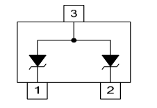
Pin Configuration
Applications
- Cellular handsets and accessories
- Personal digital assistants (PDA’s)
- Portable instrumentation
- Set Top Box (STB)
- Servers, notebook, and desktop PC
- Wireless bus protection
Page 2
Maximum Ratings
| Rating | Symbol | Value | Unit |
|---|---|---|---|
| ESD voltage (Contact discharge) | V ESD | ±8 | kV |
| ESD voltage (Air discharge) | ±15 | ||
| Storage & operating temperature range | T ,T STG J | -55~+150 | ℃ |
Electrical Characteristics (TJ=25℃)
SET23A03L02
| Parameter | Symbol | Condition | Min. | Typ. | Max. | Unit |
|---|---|---|---|---|---|---|
| Reverse stand-off voltage | V RWM | 3.3 | V | |||
| Reverse breakdown voltage | V BR | I =1mA BR | 4 | V | ||
| Reverse leakage current | I R | V =3.3V R Each I/O pin | 5 | μA | ||
| Clamping voltage (tp=8/20μs) | V C | I =1A PP | 7.5 | V | ||
| Clamping voltage (tp=8/20μs) | V C | I =10A PP | 15 | V | ||
| Off state junction capacitance | C J | 0Vdc,f=1MHz Between I/O pins and GND | 200 | pF |
SET23A05L02
| Parameter | Symbol | Condition | Min. | Typ. | Max. | Unit |
|---|---|---|---|---|---|---|
| Reverse stand-off voltage | V RWM | 5 | V | |||
| Reverse breakdown voltage | V BR | I =1mA BR | 6 | V | ||
| Reverse leakage current | I R | V =5V R Each I/O pin | 5 | μA | ||
| Clamping voltage (tp=8/20μs) | V C | I =1A PP | 9.8 | V | ||
| Clamping voltage (tp=8/20μs) | V C | I =15A PP | 20 | V | ||
| Off state junction capacitance | C J | 0Vdc,f=1MHz Between I/O pins and GND | 220 | pF |
Page 3
Electrical Characteristics (TJ=25℃)
SET23A12L02
| Parameter | Symbol | Condition | Min. | Typ. | Max. | Unit |
|---|---|---|---|---|---|---|
| Reverse stand-off voltage | V RWM | 12 | V | |||
| Reverse breakdown voltage | V BR | I =1mA BR | 13.3 | V | ||
| Reverse leakage current | I R | V =12V R Each I/O pin | 1 | μA | ||
| Clamping voltage (tp=8/20μs) | V C | I =1A PP | 19 | V | ||
| Clamping voltage (tp=8/20μs) | V C | I =10A PP | 25.9 | V | ||
| Off state junction capacitance | C J | 0Vdc,f=1MHz Between I/O pins and GND | 100 | pF |
SET23A15L02
| Parameter | Symbol | Condition | Min. | Typ. | Max. | Unit |
|---|---|---|---|---|---|---|
| Reverse stand-off voltage | V RWM | 15 | V | |||
| Reverse breakdown voltage | V BR | I =1mA BR | 16.7 | V | ||
| Reverse leakage current | I R | V =15V R Each I/O pin | 1 | μA | ||
| Clamping voltage (tp=8/20μs) | V C | I =1A PP | 24 | V | ||
| Clamping voltage (tp=8/20μs) | V C | I =10A PP | 30 | V | ||
| Off state junction capacitance | C J | 0Vdc,f=1MHz Between I/O pins and GND | 90 | pF |
SET23A24L02
| Parameter | Symbol | Condition | Min. | Typ. | Max. | Unit |
|---|---|---|---|---|---|---|
| Reverse stand-off voltage | V RWM | 24 | V | |||
| Reverse breakdown voltage | V BR | I =1mA BR | 26.7 | V | ||
| Reverse leakage current | I R | V =24V R each I/O pin | 1 | μA | ||
| Clamping voltage (tp=8/20μs) | V C | I =1A PP | 43 | V | ||
| Clamping voltage (tp=8/20μs) | V C | I =5A PP | 49 | V | ||
| Off state junction capacitance | C J | 0Vdc,f=1MHz Between I/O pins and GND | 80 | pF |
Page 4
Electrical Characteristics (TJ=25℃)
SET23A36L02
| Parameter | Symbol | Condition | Min. | Typ. | Max. | Unit |
|---|---|---|---|---|---|---|
| Reverse stand-off voltage | V RWM | 36 | V | |||
| Reverse breakdown voltage | V BR | I =1mA BR | 40 | V | ||
| Reverse leakage current | I R | V =36V R each I/O pin | 1 | μA | ||
| Clamping voltage (tp=8/20μs) | V C | I =1A PP | 51 | V | ||
| Clamping voltage (tp=8/20μs) | V C | I =5A PP | 76.8 | V | ||
| Off state junction capacitance | C J | 0Vdc,f=1MHz Between I/O pins and GND | 70 | pF |
Typical Characteristics Curves
Figure 1. Power Derating Curve
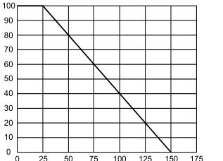
TA-Ambient Temperature (℃)
Figure 3. Forward Voltage vs. Forward Current
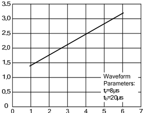
Figure 2. Pulse Waveforms
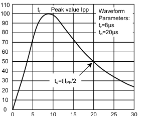
t-Time (μs)
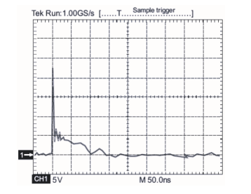
Figure 4. ESD Clamping(8kV Contact IEC61000-4-2)
Page 5
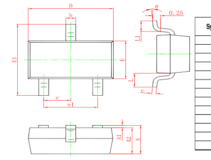
| Symbol | Dimensions In Millimeters | Dimensions In Inches | ||
|---|---|---|---|---|
| Min. | Max. | Min. | Max. | |
| A | 0.900 | 1.150 | 0.035 | 0.045 |
| A1 | 0.000 | 0.100 | 0.000 | 0.004 |
| A2 | 0.900 | 1.050 | 0.035 | 0.041 |
| b | 0.300 | 0.500 | 0.012 | 0.020 |
| c | 0.080 | 0.150 | 0.003 | 0.006 |
| D | 2.800 | 3.000 | 0.110 | 0.118 |
| E | 1.200 | 1.400 | 0.047 | 0.055 |
| E1 | 2.250 | 2.550 | 0.089 | 0.100 |
| e | 0.950 TYP. | 0.037 TYP. | ||
| e1 | 1.800 | 2.000 | 0.071 | 0.079 |
| L | 0.550 REF. | 0.022 REF. | ||
| L1 | 0.300 | 0.500 | 0.012 | 0.020 |
| θ | 0° | 8° | 0° | 8° |
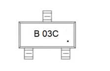
Marking
Ordering information
| Order code | Package | Baseqty | Deliverymode | Marking |
| UMW SET23A03L02 | SOT-23 | 3000 | Tape and reel | B 03C |
| UMW SET23A05L02 | SOT-23 | 3000 | Tape and reel | B 05C |
| UMW SET23A12L02 | SOT-23 | 3000 | Tape and reel | B 12C |
| UMW SET23A15L02 | SOT-23 | 3000 | Tape and reel | B 15C |
| UMW SET23A24L02 | SOT-23 | 3000 | Tape and reel | B 24C |
| UMW SET23A36L02 | SOT-23 | 3000 | Tape and reel | B 36C |