
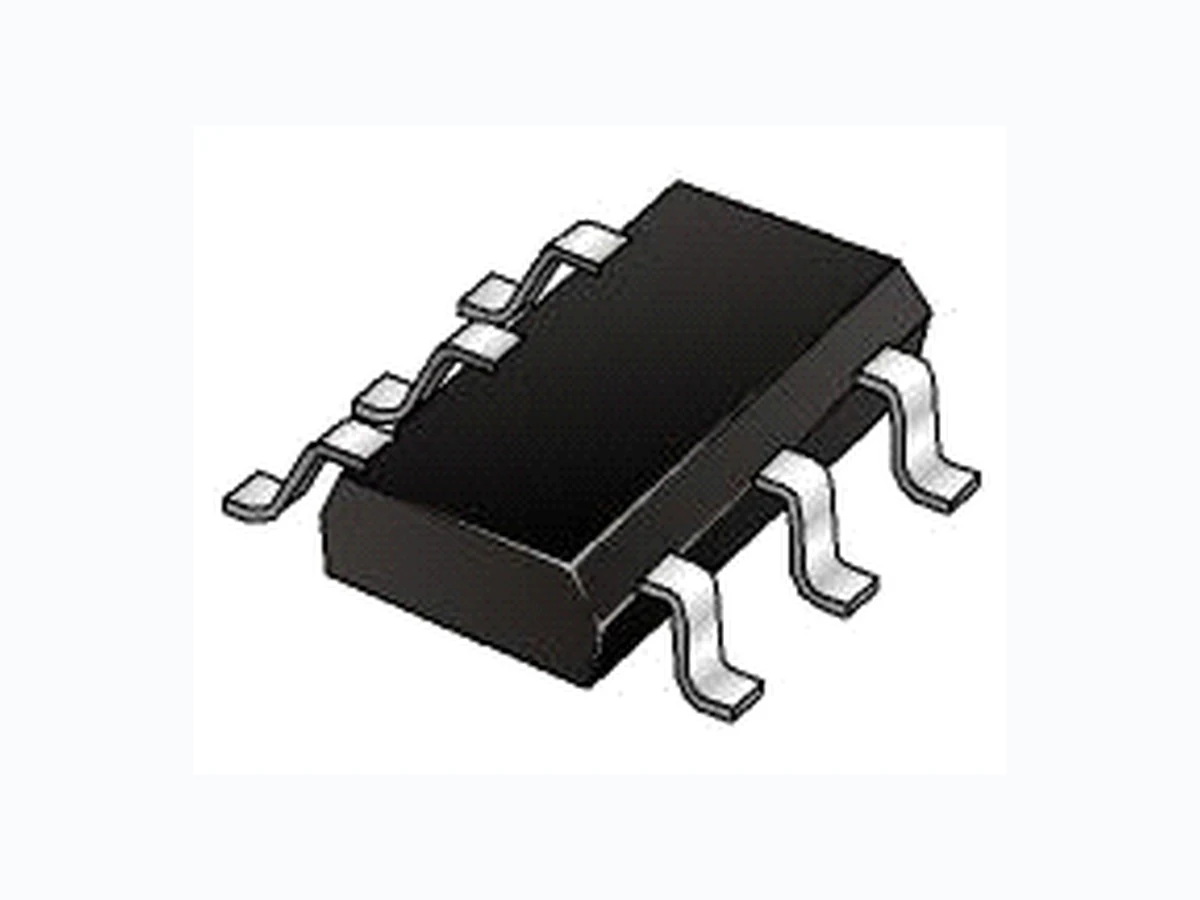
Advanced constant voltage and constant current controller
Document overview
- Manufacturer or author: STMICROELECTRONICS
- PDF pages: 10
Technical content
Features
■ Constant voltage and constant current control ■ Wide operating VCC range [3.5 - 36] V ■ Low quiescent consumption: 200 µA ■ Voltage reference: 2.5 V ■ Voltage control loop accuracy +/- 0.5% ■ Current sense threshold: 50 mV ■ Open-drain output stage ■ Low external component count ■ SOT23-6L micro package
Applications
■ Battery chargers ■ AC-DC adapters ■ LED drivers
Description
The SEA05 is a highly integrated solution for SMPS applications requiring a dual control loop to perform CV (constant voltage) and CC (constant current) regulation. The device integrates a voltage reference, two op- amps (with OR-ed open-drain outputs), and a low- side current sensing circuit. The voltage reference, along with one op-amp, is the core of the voltage control loop; the current sensing circuit and the other op-amp make up the current control loop. The external components needed to complete the two control loops are: a resistor divider that senses the output of the power supply and fixes the voltage regulation setpoint at the specified value; a sense resistor that feeds the current sensing circuit with a voltage proportional to the dc output current; this resistor determines the current regulation setpoint and must be adequately rated in terms of power dissipation; the frequency compensation components (R-C networks) for both loops. The device, housed in one of the smallest available package, is ideal for space-shrunk applications such as adapters and chargers. Figure 1. Internal schematic Table 1. Device summary
1 Pin description
Figure 2. Pin configuration accidental short circuit among pins. Table 2. Pin description current sense resistor through a decoupling resistor. Ground. Return of the bias current of the device. 0 V reference for all voltages. possible to minimize load current effect on the voltage regulation setpoint. resistor divider that senses the output voltage. transmit the error signal to the primary side.
2 Maximum ratings
3 Typical application schematic
Figure 3. Typical application schematic Table 3. Absolute maximum ratings Table 4. Thermal data
4 Electrical characteristics
Table 5. Electrical characteristics
- If the voltage on Vctrl (the negative input of the amplifie r) is higher than the positive amplifier input, and it is
increased by 1 mV, the sinking current at the output OUT is increased by 3.5 mA.
- The internal voltage reference is set at 2.5 V. Th e voltage control loop precision takes into account the
to 0.48 % accuracy at room temperature.
- When the positive input at Ictrl is lower than -50 mV, and the voltage is decreased by 1 mV, the sinking
current at the output out is increased by 7 mA.
- Considering Ictrl pin directly c onnected to the hot (negative) end of the current sense resistor and Isense
well as the input offset voltage of the transconductance operational amplifier.
5 Application information
Figure 4. Application information exceed the AMR of Ictrl pin. down to –Vo. This could damage the IC in case the Ictrl pin AMR is violated. value of the external resistor gives the current sense threshold variation.
Voltage and current control SEA05 6/10 Doc ID 17014 Rev 1
6 Voltage and current control
6.1 Voltage control
The voltage loop is controlled via a first transconductance operational amplifier, the voltage divider R1, R2, and the optocoupler which is directly connected to the output. Its possible to choose the values of R1 and R2 resistors using Equation 1-2: Equation 1 Equation 2 where Vo is the desired output voltage. As an example, with R1 = 100 kΩ and R2 = 15 kΩ Vo = 19.17 V
6.2 Current control
The current loop is controlled via the second trans-conductance operational amplifier, the sense resistor Rsense, and the optocoupler. The control equation verifies: Equation 3 Equation 4 where Iomax is the desired limited current, and Vcsth is the threshold voltage for the current control loop. As an example, with Iomax = 1 A, Vcsth = 50 mV, then Rsense = 50 m Ω. Note that the Rsense resistor should be chosen taking into account the maximum dissipation (Plim) through it during full load operation. Equation 5 As an example, with Iomax = 1 A, and Vcsth = 50 mV, Plim = 50 mW. Therefore, for most adaptor and battery charger applications, it is suitable a low power resistor to make the current sensing function. o R )RR(VctrlV +∗= Vctrl )VctrlV(RR O −∗= VcsthIR maxosense =∗ maxo sense I VcsthR = PLim Vcsth lomax⋅=
Figure 4. The resistors of this voltage divider are matched to provide the best described with a square characteristic as shown in the following V/I output-power graph. Figure 5. Output voltage versus output current
7 Compensation
components as shown in Figure 4.
8 Package mechanical data
specifications, grade definitions and product status are available at: www.st.com. ECOPACK® is an ST trademark. Figure 6. SOT23-6L package dimensions Table 6. SOT23-6L mechanical data
9 Revision history
Table 7. Document revision history 26-Apr-2010 1 Initial release.