
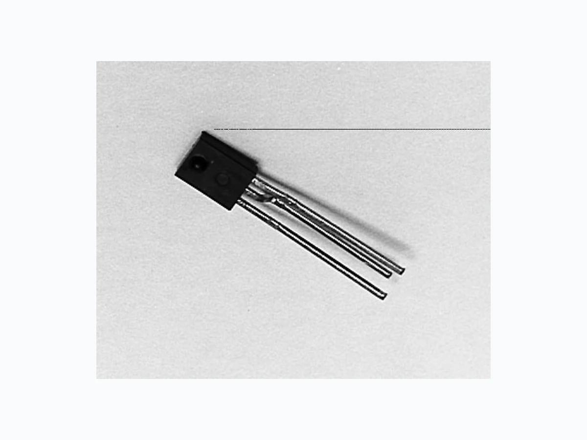
SDP8600 ETC
Document overview
- Manufacturer or author: Provided By www.digicamel.com(FREE DATASHEET DOWNLOAD SITE)
- PDF pages: 4
Technical content
DESCRIPTION
FEATURES
Side-looking plastic package• 55¡ (nominal) acceptance angle• Wide sensitivity ranges• TTL/LSTTL/CMOS compatible• Buffer (SDP8600/8601/8602) or inverting (SDP8610/8611/8612) logic available Three different lead spacing arrangements• Mechanically and spectrally matched to SEP8506 and SEP8706 infrared emitting diodes The SDP86XX series is a family of single chip Optoschmitt IC detectors molded in a side-looking black plastic package to minimize the effect of visible ambient light. The photodetector consists of a photodiode, amplifier, voltage regulator, Schmitt trigger and an NPN output transistor with a 10 kì (nominal) pull-up resistor. Output rise and fall times are independent of the rate of change of incident light. Detector sensitivity has been internally temperature compensated. Flexibility of use is enhanced by a choice of three different lead configurations; in-line (SDP8601/8611), 0.05 in.(1.27 mm) offset pin circle (SDP8600/8610) and 0.10 in. (2.54 mm) offset center lead (SDP8602/8612). Device Polarity: Buffer - Output is HI when incident light intensity is above the turnon threshold level. Inverter - Output is LO when incident light intensity is above the turnon threshold level. DIM_028.cdr INFRA--6.TIF OUTLINE DIMENSIONS in inches (mm) 3 plc decimals ±0.005(0.12)Tolerance 2 plc decimals ±0.020(0.51) Honeywell reserves the right to make changes in order to improve design and supply the best products possible.h200
ELECTRICAL CHARACTERISTICS
UNITS TEST CONDITIONSMINPARAMETER SYMBOL TYP MAX ABSOLUTE MAXIMUM RATINGS (25¡C Free-Air Temperature unless otherwise noted) Supply Voltage 12 V [À] Duration of Output Short to VÙÙ or Ground 1.0 sec Output Current 18 mA Operating Temperature Range -40¡C to 85¡C Storage Temperature Range -40¡C to 85¡C Soldering Temperature (5 sec) 240¡C Notes 1. Derate linearly from 25¡C to 5.5 V at 85¡C. SCHEMATIC Honeywell reserves the right to make changes in order to improve design and supply the best products possible. h 201
SCH_024.cdr SWITCHING TIME TEST CIRCUIT cir_007.cdr SWITCHING WAVEFORM FOR BUFFERS cir_013.cdr SWITCHING WAVEFORM FOR INVERTERS cir_011.cdr Responsivity vs Angular Displacement gra_065.ds4 Angular displacement - degrees Relative response 0.0 0.1 0.2 0.3 0.4 0.5 0.6 0.7 0.8 0.9 1.0 -60 -45 -30 -15 0 +15 +30 +45 +60 Fig. 1 Threshold Irradiance vs Temperature gra_060.ds4 Temperature - °C Relative irradiance 0.0 0.2 0.3 0.4 0.5 2.0 1.0 -40 -20 0 20 40 60 80 100 Fig. 2 Honeywell reserves the right to make changes in order to improve design and supply the best products possible.h202
Output Rise Time (t²) and Output Fall Time (t¶) vs Temperature gra_061.ds4 Temperature - °C Rise tim e (TR) & fall tim e (TF) - ns 100 120 140 160 180 220 240 -40 -20 0 20 40 60 80 100
200 Symbol definition & test
Fig. 3 Delay Time vs Temperature gra_062.ds4 Ambient temperature - °C Propagation delay - µs 0.0 1.4 1.8 2.2 2.6 3.0 3.4 3.8 4.2 -40 -20 0 20 40 60 80 100 TPLH TPHL Fig. 4 Spectral Responsivity gra_050.ds4 Wavelength - nm Relative response 0.0 0.1 0.2 0.3 0.4 0.5 0.6 0.7 0.8 0.9 1.0 600 700 800 900 1000 1100 1200 Fig. 5 All Performance Curves Show Typical Values Honeywell reserves the right to make changes in order to improve design and supply the best products possible. h 203