


 Download PDF
SDD32A05L01 UMW
Document overview
- PDF pages: 3
Technical content
Page 1
Description
DESCRIPTION
The UMW SDD32A05L01 is designed to protect low voltage sensitive components from ESD and transient voltage events. Excellent clamping capability, low leakage, and fast response time, make these parts ideal for ESD protection on designs where board space is at a premium. Because of its small size, it is suited for use in cellular phones, portable devices, digital cameras, power supplies and many other portable applications.It is designed to protect sensitive semiconductor components from damage or upset due to electrostatic discharge(ESD), electrical fast transients(EFT), and cable discharge events(CDE).
FEATURES
- IEC61000-4-2 ESD 15KV Air, 8KV contact compliance
- SOD-323 surface mount package
- Protects one I/O line
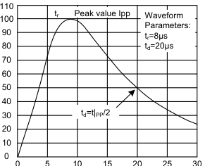
- Peak power dissipation of 320W under 8/20μs waveform
- Working voltage: 5V
- Low leakage current
- Low clamping voltage
- Solid-state silicon avalanche technology
- Lead Free/RoHS compliant
- Solder reflow temperature: Pure Tin-Sn, 260~270℃
- Flammability rating UL 94V-0
- Marking: 05W
MAXIMUM RATINGS
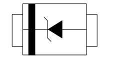
APPLICATIONS
- Cellular handsets & Accessories
- Cordless phones
- Personal digital assistants (PDAs)
- Notebooks & Handhelds
- Portable instrumentation
- Digital cameras
- Peripherals
- MP3 players
| Rating | Symbol | Value | Unit |
|---|---|---|---|
| Peak pulse power (tp=8/20μs waveform) | P PP | 320 | W |
| ESD voltage (Contact discharge) | V ESD | ±8 | kV |
| ESD voltage (Air discharge) | ±15 | ||
| Storage & operating temperature range | T ,T STG J | -55~+150 | ℃ |
Page 2
| Parameter | Symbol | Condition | Min. | Typ. | Max. | Unit |
|---|---|---|---|---|---|---|
| Reverse stand-off voltage | V RWM | 5 | V | |||
| Reverse breakdown voltage | V BR | I =1mA BR | 6 | V | ||
| Reverse leakage current | I R | V =5V R | 10 | μA | ||
| Clamping voltage (tp=8/20μs) | V C | I =1A PP | 9.8 | V | ||
| Clamping voltage (tp=8/20μs) | V C | I =24A PP | 20 | V | ||
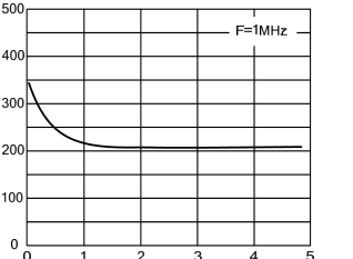
| Off state junction capacitance | C J | 0Vdc,f=1MHz | 350 | pF |
TYPICAL CHARACTERISTICS CURVES
Figure 2. Pulse Waveform
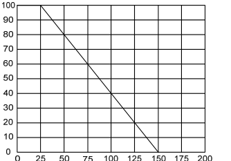
Figure 1. Power Derating Curve
t-Time (μs)
Figure 3. Capacitance vs. Reverse Voltage
Page 3
Description
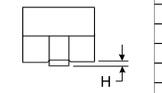
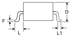
Outline Drawing – SOD-323
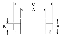
| DIMENSIONS | ||||
| SYMBOL | MILLIMETER | INCHES | ||
| MIN | MAX | MIN | MAX | |
| A | 1.600 | 1.800 | 0.063 | 0.071 |
| B | 0.250 | 0.350 | 0.010 | 0.014 |
| C | 2.500 | 2.700 | 0.098 | 0.106 |
| D | 1.000 | 0.039 | ||
| E | 1.200 | 1.400 | 0.047 | 0.055 |
| F | 0.080 | 0.150 | 0.003 | 0.006 |
| L | 0.475 REF | 0.019REF | ||
| L1 | 0.250 | 0.400 | 0.010 | 0.016 |
| H | 0.000 | 0.100 | 0.000 | 0.004 |
Marking
Ordering information
| Order code | Package | Baseqty | Deliverymode |
| UMW SDD32A05L01 | SOD-323 | 3000 | Tape and reel |