
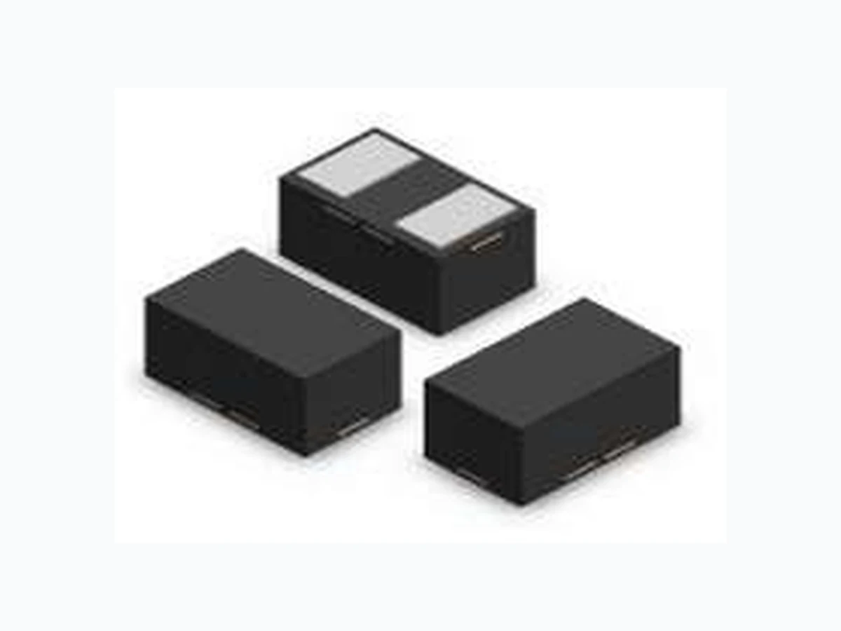
SDA3011CDN LEIDITECH
Document overview
- Manufacturer or author: Provided By www.digicamel.com(FREE DATASHEET DOWNLOAD SITE)
- PDF pages: 4
Technical content
Features
- Ultr a low leakage: nA level
- Operatin g voltage: 30V
- Low clam ping voltage
- Complies w ith following standards: – IEC 61000-4-2 (ESD) immunity test Air discharge: ±25kV Contact discharge: ±15KV – IEC61000-4-4 (EFT) 40A (5/50ns) – IEC61000-4-5 (Lightning) 3A (8/20μs)
- RoHS Co mpliant Ap plications Dimensio ns DFN1006 Mechanical Characteristics
- Package: DFN1006
- Lead Fi nish: Lead Free
- UL F lammability Classification Rating 94V-0
- Quantity Per Reel:10,000pcs
- Ree l Size:7 inch Ab solute Maximum Ratings(Tamb =25°C unless otherwise specified) Para meter Symbol Value Unit Peak Pul se Power (8/20µs) Ppp 171 W ESD per IEC 61000−4−2 (Air) VESD ± 25 Kv ESD per IEC 61000−4−2 (Contact) ± 15 Operating Temperature Range TJ -40 to +125 ℃ Storag e Temperature Range TSTJ -55 to +150 ℃ Cellular Handsets & Accessories Keypads, Side keys, Audio Ports Portable Instrumentation Notebooks, Desktops, and Servers Digital Lines Tablet PC Rev 2.0 : www.leiditech.com12.01.2019 1/4
- Device Marking:DL 1-Line Bi-directional TVS Diode Typic Application Schema tic Pin Conf iguration
l Characteristics(T A=25°C unless otherwise specified) Rev P arameter Symbol Min Typ Max Unit Test Condition Reverse Working Voltage VRWM 30 V Breakdown Voltage VBR 30.8 V IT = 1mA Reverse Leakage Current IR 1 µA VRWM = 30V Clamping Voltage VC 57 V IPP = 3A (8 x 20 s pulse) Junction Capacitance CJ 16 pF V = 0V, f = 1MHz μ R 33.7 37 Typical Characteristics F ig1. 8/20 µs Pulse Waveform 5 10 15 20 25 30 120 tr Pe ak Value IP P td= t IPP/ T EST WAVEFORM PARAMETERS t 8 s td= 20 s t - Time (s IPP - Peak Pulse Current - % of IPP F ig3. Power Derating Curve 25 50 75 100 125 150 110 100 of Rated Power Am bient Temperature–TA (ºC F ig2. ESD Pulse Waveform (according to IEC 61000-4-2) 60n s 10% P ercent of Peak Pulse Current % 30n s tr = 0.7~1ns Time (ns) 90% 100% SDA3011CDN
T ransmission Line Pulse (TLP) is a measurement technique used in the Electrostatic Discharge (ESD) arena to characterize performance attributes of devices under ESD stresses. TLP is able to obtain current versus voltage (I−V) curves in which each data point is obtained with a 100 ns long pulse, with currents up to 40 A. TLP was first used in the ESD field to study human body model (HBM) in integrated circuits, but it is an equally valid tool in the field of system level ESD. The applicability of TLP to system level ESD is illustrated in Figure 1, which compares an 8 kV IEC 61000−4−2 current waveform with TLP current pulses of 8 and 16 A. The current levels and time duration for the pulses are similar and the initial rise time for the TLP pulse is comparable to the rise time of the IEC 61000−4−2’s initial current spike. This application note will give a basic introduction to TLP measurements and explain the datasheet parameters extracted from TLP for SDI Technology’s protection products. C omparison of a CurrentWaveform of IEC 61000 −4−2w ith TLP Pulses at 8 and 16 A. The IEC 61000−4−2 ESD waveforms is true to the Standard and is shown here as captured on an oscilloscope. The points A, B, and C show the points on the aveforms specified in IEC 61000−4−2. Transmission Line Pulse (TLP) Version. Transm ission Line Pulse (TLP) Comparison Between 8 kV IEC 61000−4−2 and 8 A and 16 A TLP Waveforms SDA3011CDN
DFN1006 PACKAGE OUTLINE & DIMENSIONS Suggested Land Pattern SYM DIMENSIONS MILLIMETERS INCHES MIN NOM MAX MIN NOM MAX e 0.65 BSC 0.026 BSC SYM DIMENSIONS MILLIMETERS INCHES X 0.60 0.024 Y1 0.50 0.020 Y2 0.30 0.012 Y3 0.80 0.032 Z 1.30 0.052 E - D L b - e h h A c Bottom View Y2Y3 X Z Sha nghai Leiditech Electronic Co.,Ltd Email: sale1@leiditech.com Tel : +86- 021 50828806 Fax : +86- 021 50477059 Rev SDA3011CDN