
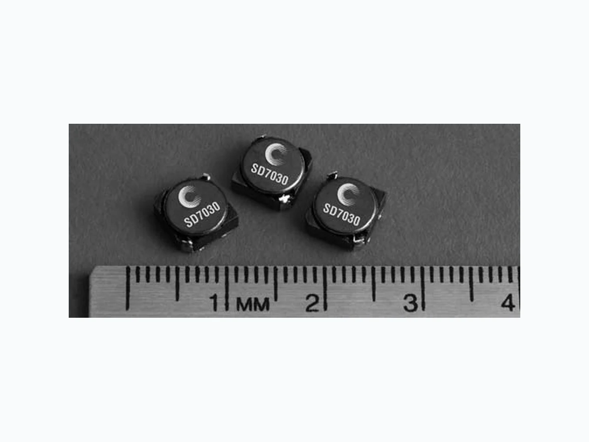
SD7030-3R3-R ETC2
Document overview
- Manufacturer or author: Provided By www.digicamel.com(FREE DATASHEET DOWNLOAD SITE)
- PDF pages: 4
Technical content
Applications
- Notebook computers Wireless handsets TFT LCD Bias supplies GPS Receivers Handheld instruments ADSL/DSL/Cable modems Battery power, Li-lon, 2-cell Digital still camera White LED driver Buck and boost inductor Environmental Data Storage temperature range: -40°C to +125°C Operating temperature range: -40°C to +125°C (ambient plus self-temperature rise) Solder reflow temperature: J-STD-020D compliant Packaging Supplied in tape and reel packaging, 1500 parts per 13” diameter. reel Low-Profile Shielded Drum Inductors SD7030 Series
1011 BU-SB111167 Page 1 of 4 Data Sheet: 4330
1 Open Circuit Inductance Test Parameters: 100kHz, 0.1V, 0.0Adc. 2I rms: DC current for an approximate ΔT of 40°C without core loss. Derating is necessary for AC currents. PCB layout, trace thickness and width, air-flow, and proximity of other heat generating components will affect the temperature rise. It is recommended that the temperature of the part not exceed 125°C under worst case operating conditions verified in the end application. 3I sat Amps peak for approximately 35% rolloff (@25°C) 4 K-factor: Used to determine Bp-p for core loss (see graph). Bp-p = K*L*ΔI, Bp-p(mT), K: (K factor from table), L: (Inductance in μH), ΔI (Peak-to-peak ripple current in Amps).
5 Part Number Definition: SD7030-xxx-R
SD7030 = Product code and size; -xxx = Inductance value in μH; R = decimal point; If no R is present, third character = # of zeros. -R suffix = RoHS compliant Product Specifications Part Number5 OCL1 μH ± 30% I rms
2 Amps I sat
3 Amps Typ. DCR m Ω @ 25°C Max DCR m Ω @ 25°C K-factor 4 SD7030-1R5-R 1.5 5.5 4.5 10 12 32 SD7030-3R3-R 3.3 3.7 3.00 20 24 22 SD7030-3R9-R 4.1 3.4 2.60 22 27 19 SD7030-5R0-R 4.9 3.2 2.40 26 31 17 SD7030-6R0-R 5.8 2.8 2.25 29 35 16 SD7030-7R3-R 7.0 2.3 2.10 45 54 13 SD7030-8R0-R 7.8 2.2 1.85 48 58 12 SD7030-100-R 10.0 2.1 1.70 54 65 11 SD7030-120-R 11.5 1.9 1.55 58 70 10 SD7030-150-R 14.6 1.7 1.40 70 84 9.3 SD7030-180-R 17.3 1.7 1.32 79 95 8.8 SD7030-220-R 21.0 1.4 1.20 107 128 7.6 SD7030-260-R 24.9 1.3 1.05 118 142 6.9 SD7030-300-R 30.0 1.2 0.97 138 165 6.4 SD7030-390-R 39.7 1.1 0.86 175 210 5.7 SD7030-440-R 43.4 1.1 0.80 198 238 5.3 SD7030-560-R 54.4 0.99 0.73 231 277 4.9 SD7030-680-R 66.6 0.85 0.65 253 304 4.3 SD7030-820-R 81.4 0.82 0.60 325 390 4.0 SD7030-101-R 95.5 0.70 0.54 446 535 3.6 SD7030-121-R 115.2 0.67 0.50 629 755 3.3 SD7030-151-R 145 0.57 0.44 715 858 2.9 SD7030-181-R 174 0.54 0.40 805 966 2.7 SD7030-221-R 211 0.51 0.36 1102 1322 2.4 SD7030-271-R 264 0.44 0.33 1259 1475 2.2 SD7030-331-R 317 0.38 0.30 1438 1725 2.0 SD7030-391-R 381 0.36 0.27 1857 2228 1.8 SD7030-471-R 460 0.34 0.25 2150 2581 1.7 SD7030-561-R 561.0 0.29 0.23 2857 3428 1.5 SD7030-681-R 677.2 0.28 0.21 3206 3847 1.4
Description
125°C maximum total operating temperature Low profile 7.0 x 7.0 x 3.0mm maximum surface mount package Ferrite material shielded drum core Inductance range from 1.5µH to 680µH Current range from 0.21 to 5.5 Amps Frequency range up to 1MHz Pb HALOGEN HFFREE
Top View Bottom View Front View Recommended Pad Layout Schematic Left View 1MHz 500kHz 300kHz 100kHz 200kHz Part Marking: Coiltronics Logo xxx = inductance value in μH. R = decimal point. If no “R” is present, third character = # of zeros. wwlly or wwllyy = date code. R = revision level Supplied in tape-and-reel packaging, 1500 parts per reel, 13” diameter reel. Packaging Information - mm Core Loss
1011 BU-SB111167 Page 2 of 4 Data Sheet: 4330
1011 BU-SB111167 Page 3 of 4 Data Sheet: 4330
-40°C +25°C +85°C Inductance Characteristics Temperature Rise vs. Loss
The only controlled copy of this Data Sheet is the electronic read-only version located on the Cooper Bussmann Network Drive. A ll other copies of this document are by definition uncon- trolled. This bulletin is intended to clearly present comprehensive product data and provide technical information that will he lp the end user with design applications. Cooper Bussmann reserves the right, without notice, to change design or construction of any products and to discontinue or limit distribution o f any products. Cooper Bussmann also reserves the right to change or update, without notice, any technical information contained in this bulletin. Once a product has been selected, it sh ould be tested by the user in all possible applications. Life Support Policy: Cooper Bussmann does not authorize the use of any of its products for use in life support devices or systems without the express written approval of an officer of the Company. Life support systems are devices which support or sustain life, and whose failure to perform, when properly used in ac cordance with instructions for use provided in the label- ing, can be reasonably expected to result in significant injury to the user. North America Cooper Electronic Technologies
1225 Broken Sound Parkway NW
Boca Raton, FL 33487-3533 Tel: 1-561-998-4100 Fax: 1-561-241-6640 Toll Free: 1-888-414-2645 Cooper Bussmann P .O. Box 14460 St. Louis, MO 63178-4460 Tel: 1-636-394-2877 Fax: 1-636-527-1607 Europe Cooper Electronic Technologies Cooper (UK) Limited Burton-on-the-Wolds Leicestershire • LE12 5TH UK Tel: +44 (0) 1509 882 737 Fax: +44 (0) 1509 882 786 Cooper Electronic Technologies Avda. Santa Eulalia, 290 08223 Terrassa, (Barcelona), Spain Tel: +34 937 362 812 +34 937 362 813 Fax: +34 937 362 719 Asia Pacific Cooper Electronic Technologies
1 Jalan Kilang Timor
#06-01 Pacific Tech Centre Singapore 159303 Tel: +65 278 6151 Fax: +65 270 4160 © 2011 Cooper Bussmann www.cooperbussmann.com
1011 BU-SB111167 Page 4 of 4 Data Sheet: 4330
t tP ts TC -5°C Time 25°C to Peak Time 25°C Tsmin Tsmax TL TP Preheat A Max. Ramp Up Rate = 3°C/s Max. Ramp Down Rate = 6°C/s TTaabbllee 11 -- SSttaannddaarrdd SSnnPPbb SSoollddeerr ((TTcc)) Volume Vol ume Packagem m 3 mm3 Thickness <350 > _350 <2.5mm 235° C 220°C >_2.5mm 220° C 220°C TTaabbllee 22 -- LLeeaadd ((PPbb)) FFrreeee SSoollddeerr ((TTcc)) Volume Vol ume Vol ume Packagem m 3 mm3 mm3 Thickness <350 350 - 2000 >2000 <1.6mm 2 60°C 260°C 260°C 1.6 – 2.5mm 2 60°C 250°C 245°C >2.5mm 250° C 245°C 245°C Reference JDEC J-STD-020D Profile Feature Standard SnPb Solder Lea d (Pb) Free Solder Preheat and Soak T emperature min. (Tsmin) 100° C 150°C Temperature max. (Tsmax) 150° C 200°C Time (Tsmin to Tsmax) (ts) 60-120 Seconds 60-120 Seconds Average ramp up rate Tsmax to Tp 3°C/ Second Max. 3° C/ Second Max. Liquidous temperature (TL) 183° C 217°C Time at liquidous (tL) 60-150 Seconds 60-150 Seconds Peak package body temperature (TP)* Table 1T able 2 Time (tp) within 5 °C of the specified classification temperature (Tc) 20 Seconds 30 Seconds** Average ramp-down rate (Tp to Tsmax) 6°C/ Second Max. 6°C/ Second Max. Time 25°C to Peak Temperature6 Minutes Max. 8 Minut es Max. * Tolerance for peak profile temperature (Tp) is defined as a supplier minimum and a user maximum. ** Tolerance for time at peak profile temperature (tp) is defined as a supplier minimum and a user maximum.