
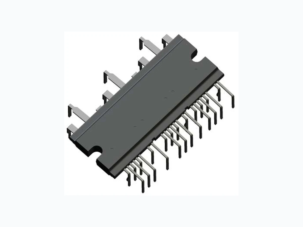
SCM1106M ALLEGRO
Document overview
- Manufacturer or author: Provided By www.digicamel.com(FREE DATASHEET DOWNLOAD SITE)
- PDF pages: 10
Technical content
▪ Each half-bridge circuit consists of a pre-driver circuit that is completely independent from the others ▪ Protection against simultaneous high- and low-side turning on ▪ Bootstrap diodes with series resistors for suppressing inrush current are incorporated ▪ CMOS compatible input (3.3 to 5 V) ▪ Designed to minimize simultaneous current through both high- and low-side IGBTs by optimizing gate drive resistors ▪ UVLO protection with auto restart ▪ Overcurrent protection with off-time period adjustable by an external capacitor ▪ Fault (FO indicator) signal output at protection activation: UVLO (low side only), OCP, and STP ▪ Proprietary power DIP package High Voltage 3 Phase Motor Driver Functional Block Diagram Package: Power DIP Not to scale CFO Drive Circuit UV Detect Drive Circuit Level Shift Input Logic Shoot Through Prevention UV Detect O. C. Protect HVIC HO LO FO COM LIN HIN VCC VB HS VBB U, V, or W LS Figure 1. Diagram of one of three phases in the device.
Description
The SCM1106M inverter power module (IPM) device provides a robust, highly-integrated solution for optimally controlling 3-phase motor power inverter systems and variable speed control systems used in energy-conserving designs to drive motors of residential and commercial appliances. These ICs take 85 to 253 V AC input voltage, and 10 A (continuous) output current. They can withstand voltages of up to 600 V (IGBT breakdown voltage). The SCM1100M series employs a new, small-footprint proprietary DIP package. The IC itself consists of all of the necessary power elements (six IGBTs), pre-drive ICs (three), and flyback diodes (six), needed to configure the main circuit of an inverter, as well as a bootstrap circuit (three bootstrap diodes and three boot resistors) as a high-side drive power supply. This enables the main circuit of the inverter to be configured with fewer external components than traditional designs. Applications include residential white goods (home appliances) and commercial appliance motor control, such as: ▪ Air conditioner fan motor ▪ Refrigerator compressor motor ▪ Washing machine main motor ▪ Air conditioner compressor motor 38110.010, Rev. 2
High Voltage 3 Phase Motor DriverSCM1106M All performance characteristics given are typical values for circuit or system baseline design only and are at the nominal operating voltage and an ambient temperature, T A, of 25°C, unless oth er wise stated. Selection Guide Part Number Packing IGBT Breakdown Voltage, VCES(min) (V) IGBT Saturation Voltage, VCE(sat)(typ) (V) Output Current Continuous, IO(max) (A) Pulsed, IOP (max) (A) SCM1106M 10 pieces per tube 600 2.2 10 20 Absolute Maximum Ratings, valid at TA = 25°C Characteristic Symbol Remarks Rating Units IGBT Breakdown Voltage V CES VCC = 15 V, IC = 1 mA, VIN = 0 V 600 V Logic Supply Voltage V CC Between VCC and COM 20 V Boot-strap Voltage V BS Between VB and HS (U,V,W) 20 V Output Current, Continuous I O TCase = 25°C 10 A TCase = 100°C 5.2 A Output Current, Pulsed I OP Pulse Width ≤ 100 μs2 0 A Input Voltage V IN –0.5 to 7 V FO Terminal Voltage V FO Between FO and COM 7 V Maximum Allowable Power Dissipation P D TCase = 25°C, 1 element operation (IGBT) 20.8 W TCase = 100°C, 1 element operation (IGBT) 8.3 W Thermal Resistance, Junction-to-Case R θJC 1 element operation (IGBT) 6 °C/W 1 element operation (FWD) 6.5 °C/W Case Operation Temperature T COP –20 to 100 °C Junction Temperature (IGBT) T J 150 °C Storage Temperature T stg –40 to 150 °C Isolation Voltage V iso Between exposed tab region and each pin; 1 minute, AC 2000 V rms Recommended Operating Conditions Characteristic Symbol Remarks Min. Typ. Max. Units Main Supply Voltage V BB Between VBB and LS – 300 450 V Logic Supply Voltage V CC Between VCC and COM 13.5 – 16.5 V Logic Supply Voltage V BS Between VB and HS 13.5 – 16.5 V Minimum Input Pulse Width tINmin(on) 0.5 – – μs tINmin(off) 0.5 – – μs Dead Time t dead 1.5 – – μs Junction Temperature T J – – 125 °C Allegro MicroSystems, Inc.
115 Northeast Cutoff, Box 15036
Worcester, Massachusetts 01615-0036 (508) 853-5000 www.allegromicro.com
High Voltage 3 Phase Motor DriverSCM1106M SCM 1106 M Co n t r o l l e r VBB VCC RS CFO RFO Drive Circuit UV Detect Drive Circuit Level Shift Input Logic Shoot Through Prevention UV Detect O.C. Protect HVIC 1 Drive Circuit UV Detect Drive Circuit Level Shift Input Logic Shoot Through Prevention UV Detect O.C. Protect HVIC 2 Drive Circuit UV Detect Drive Circuit Level Shift Input Logic Shoot Through Prevention UV Detect O.C. Protect HVIC 3 CN VFO M CBOOT1 HO HS1 LO LS1 U VBB VB1 VCC1 HIN1 LIN1 COM1 FO1 CFO1 CBOOT2 HO HS2 LO LS2 V VBB VB2 VCC2 HIN2 LIN2 COM2 FO2 CFO2 CBOOT3 HO HS3 LO LS3 W VBB VB3 VCC3 HIN3 LIN3 COM3 FO3 CFO3 NOTE: ▪ All of the input pins are connected to GND with internal pull-down resistors rated at 100 k Ω, however, an external pull-down resistor may be required to secure stable condition of the inputs if high impedance conditions are applied to them. ▪ To use the OCP circuit, an external shunt resistor, RS, is needed. The RS value can be obtained from the formula: RS(Ω) = 0.5 V / Overcurrent Detection Set Current (A) . ▪ A blanking timer is built-in to mask the noise generated on RS at turn-on. ▪ The external electrolytic capacitors should be placed as close to the IC as possible, in order to avoid malfunctions from external noise interference. Put a ceramic capacitor in parallel with the electrolytic capacitor if further reduction of noise susceptibility is necessary. Typical Application Diagram Allegro MicroSystems, Inc. Worcester, Massachusetts 01615-0036 (508) 853-5000 www.allegromicro.com
High Voltage 3 Phase Motor DriverSCM1106M Input Output Truth Table HIN LIN OUT L L High Z LHL HLH H H High Z High Z = High Impedence ELECTRICAL CHARACTERISTICS, valid at T A=25°C, unless otherwise noted Characteristics Symbol Conditions Min Typ Max Units Logic Supply Voltage V CC Between VCC and COM 13.5 – 16.5 V Logic Supply Current I CC VCC = 15 V, 3 phases operating – 5 8 mA Input Voltage VIH VCC = 15 V, output on – 2.0 2.5 V VIL VCC = 15 V, output off 1.0 1.5 – V Input Voltage Hysteresis V Ihys VCC = 15 V – 0.5 – V Input Current IIHH VCC = 15 V, VIN = 5 V – 50 100 μA IILH VCC = 15 V, VIN = 0 V – – 2 μA Undervoltage Lock Out (High Side) UVHL VCC = 15 V 10.0 – 12.0 V UVHH 10.5 – 12.5 V Undervoltage Lock Out (Low Side) UVLL VCC = 15 V 10.5 – 12.5 V UVLH 11.0 – 13.0 V FO Terminal Output Voltage VFOL VCC = 15 V, VFO = 5 V, RF=10 kΩ – – 0.5 V VFOH 4.8 – – V Overcurrent Protection Trip Voltage V TRIP VCC = 15 V 0.46 0.50 0.54 V Overcurrent Protection Hold Time t p VCC = 15 V, CFO = 0.022 μF2 – – m s Blanking Time t blank VCC = 15 V – 2 – μs IGBT Breakdown Voltage V CES VCC = 15 V, IC = 250 μA, VIN = 0 V 600 – – V IGBT Leakage Current I CES VCC = 15 V, VCE = 600 V, VIN = 0 V – – 1 mA IGBT Saturation Voltage V CE(sat) VCC = 15 V, IC =10 A, VIN = 5 V – 2.2 2.6 V Diode Forward Voltage V F VCC = 15 V, IF = 10 A, VIN = 0 V – 1.8 2.2 V Diode Recovery Time t rr IF = 10 A, di / dt = 100 A/μs – 50 – ns Diode Leakage Current (Boot Strap) I Lb VR = 600 V – 5 10 μA Diode Forward Voltage (Boot Strap) V Fb IF = 0.15 A – 1.1 1.3 V Diode Series Resistor (Boot Strap) R b 17.6 22.0 26.4 Ω High Side Switching Time tdH(on) VBB = 300 V, VCC = 15V, IC =10 A, inductive load; VIN 0→5 V or 5→0 V – 0.42 – μs trH – 0.09 – μs tdH(off) – 0.53 – μs tfH – 0.07 – μs Low Side Switching Time tdL(on) – 0.49 – μs trL – 0.15 – μs tdL(off) – 0.62 – μs tfL – 0.06 – μs Allegro MicroSystems, Inc. Worcester, Massachusetts 01615-0036 (508) 853-5000 www.allegromicro.com
High Voltage 3 Phase Motor DriverSCM1106M Pin-out Diagram Branded Side 3325 124 Terminal List Table Name Number Function
1 FO1 U phase fault output for overcurrent and UVLO detected
2 CFO1 Capacitor for U phase overcurrent protection hold time
3 LIN1 Signal input for low-side U phase (active high)
4 COM1 Supply ground for U phase IC
5 HIN1 Signal input for high-side U phase (active high)
6 VCC1 Supply voltage for U phase IC
7 VB1 High-side floating supply voltage for U phase
8 HS1 High-side floating supply ground for U phase
9 FO2 V phase fault output for overcurrent and UVLO detected
10 CFO2 Capacitor for V phase overcurrent protection hold time
11 LIN2 Signal input for low-side V phase (active high)
12 COM2 Supply ground for V phase IC
13 HIN2 Signal input for high-side V phase (active high)
14 VCC2 Supply voltage for V phase IC
15 VB2 High-side floating supply voltage for V phase
16 HS2 High-side floating supply ground for V phase
17 FO3 W phase fault output for overcurrent and UVLO detected
18 CFO3 Capacitor for W phase overcurrent protection hold time
19 LIN3 Signal input for low-side W phase (active high)
20 COM3 Supply ground for W phase IC
21 HIN3 Signal input for high-side W phase (active high)
22 VCC3 Supply voltage for W phase IC
23 VB3 High-side floating supply voltage for W phase
24 HS3 High-side floating supply ground for W phase
25 VBB Positive dc bus supply voltage
26 W Output for W phase
27 LS3 Negative dc bus supply ground for W phase
28 VBB Cut-pin ( positive dc bus supply voltage)
29 V Output for V phase
30 LS2 Negative dc bus supply ground for V phase
31 VBB Cut-pin ( positive dc bus supply voltage)
32 U Output for U phase
33 LS1 Negative dc bus supply ground for U phase
Allegro MicroSystems, Inc. Worcester, Massachusetts 01615-0036 (508) 853-5000 www.allegromicro.com
High Voltage 3 Phase Motor DriverSCM1106M Timing Diagrams HIN LIN VB -HS HO LO FO UVHL UVHH *Start from positive edge after UVLO release . CC =1 5V * No output at H-side UVLO HIN LIN VCC HO LO FO UVLL UVLH *V B -H S= 1 5V *Start from positive edge after UVLO release HIN LIN HO LO FO *VCC ,VB- HS = 15 V *While both HIN and LIN are in high state HO and LO turn off and FO signals out VCC LIN VB-HS LS FO VCC BlankingTime (2 μs typ.) CFO OCP Assist Timer (2 μs min.) Vrc (3.5 V typ.) The slope depends on CFO capacitance * Off operation of all phases can be done by wired OR system with the three FO pins short circuited IGBT turns off softly after overcurrent condition is detected Hside-Driver I/O Timing Diagrams Lside-Driver I/O Timing Diagrams Shoot Through Prevention Overcurrent Protection High-Side Driver Input/Output Low-Side Driver Input/Output Shoot-Through Prevention Overcurrent Protection Allegro MicroSystems, Inc. Worcester, Massachusetts 01615-0036 (508) 853-5000 www.allegromicro.com
High Voltage 3 Phase Motor DriverSCM1106M Leadform: 2551 Dimensions in millimeters Branding codes (exact appearance at manufacturer discretion ) 1st line, type: SCM1106M 2nd line, lot: YMDDT Where: Y is the last digit of the year of manufacture M is the month ( 1 to 9, O, N, D) DD is the date T is the tracking number Pin pitch measured at root (Bottom View) Branding Area PACKAGE OUTLINE DRAWING Leadframe plating Pb-free. Device composition complies with the RoHS directive. Allegro MicroSystems, Inc. Worcester, Massachusetts 01615-0036 (508) 853-5000 www.allegromicro.com
High Voltage 3 Phase Motor DriverSCM1106M PACKING SPECIFICATION Maximum 10 pieces per tube (pins aligned along X direction) Maximum 5 tubes in Y direction Maximum 5 tubes in Z direction Maximum pieces per carton: 10 pieces per tube 5 rows of tubes x 5 layers of tubes 250 pieces per carton Dimensions in millimeters Allegro MicroSystems, Inc. Worcester, Massachusetts 01615-0036 (508) 853-5000 www.allegromicro.com
High Voltage 3 Phase Motor DriverSCM1106M WARNING — These devices are designed to be operated at lethal voltages and energy levels. Circuit designs that embody these components must conform with applicable safety requirements. Pre cau tions must be taken to prevent accidental contact with power-line potentials. Do not connect ground ed test equipment. The use of an isolation transformer is recommended during circuit development and breadboarding. Because reliability can be affected adversely by improper storage environments and handling methods, please observe the following cautions. Cautions for Storage
- Ensure that storage conditions comply with the standard temperature (5°C to 35°C) and the standard relative humidity (around 40 to 75%); avoid storage locations that experience extreme changes in temperature or humidity.
- Avoid locations where dust or harmful gases are present and avoid direct sunlight.
- Reinspect for rust on leads and solderability of products that have been stored for a long time. Cautions for Testing and Handling When tests are carried out during inspection testing and other standard test periods, protect the products from power surges from the testing device, shorts between adjacent products, and shorts to the heatsink. Remarks About Using Silicone Grease with a Heatsink
- When silicone grease is used in mounting this product on a heatsink, it shall be applied evenly and thinly. If more silicone grease than required is applied, it may produce stress.
- Volatile-type silicone greases may permeate the product and produce cracks after long periods of time, resulting in reduced heat radiation effect, and possibly shortening the lifetime of the product.
- Our recommended silicone greases for heat radiation purposes, which will not cause any adverse effect on the product life, are indicated below: Type Suppliers G746 Shin-Etsu Chemical Co., Ltd. YG6260 GE Toshiba Silicone Co., Ltd. SC102 Dow Corning Toray Silicone Co., Ltd. Heatsink Mounting Method Torque When Tightening Mounting Screws. The recommended tightening torque for this product package type is: 58.8 to 78.4 N•cm (6.0 to 8.0 kgf•cm). Soldering
- When soldering the products, please be sure to minimize the working time, within the following limits: 260±5°C 10 s 380±5°C 5 s
- Soldering iron should be at a distance of at least 1.5 mm from the body of the products Electrostatic Discharge
- When handling the products, operator must be grounded. Grounded wrist straps worn should have at least 1 MΩ of resistance to ground to prevent shock hazard.
- Workbenches where the products are handled should be grounded and be provided with conductive table and floor mats.
- When using measuring equipment such as a curve tracer, the equipment should be grounded.
- When soldering the products, the head of soldering irons or the solder bath must be grounded in other to prevent leak voltages generated by them from being applied to the products.
- The products should always be stored and transported in our shipping containers or conductive containers, or be wrapped in aluminum foil. Allegro MicroSystems, Inc.
Worcester, Massachusetts 01615-0036 (508) 853-5000 www.allegromicro.com
High Voltage 3 Phase Motor DriverSCM1106M The products described herein are manufactured in Ja pan by Sanken Electric Co., Ltd. for sale by Allegro MicroSystems, Inc. Sanken and Allegro reserve the right to make, from time to time, such de par tures from the detail spec i fi ca tions as may be re quired to per mit im- prove ments in the per for mance, reliability, or manufacturability of its prod ucts. Therefore, the user is cau tioned to verify that the in for ma tion in this publication is current before placing any order. When using the products described herein, the ap pli ca bil i ty and suit abil i ty of such products for the intended purpose shall be reviewed at the users responsibility. Although Sanken undertakes to enhance the quality and reliability of its prod ucts, the occurrence of failure and defect of semi con duc tor products at a certain rate is in ev i ta ble. Users of Sanken products are requested to take, at their own risk, preventative measures including safety design of the equipment or systems against any possible injury, death, fires or damages to society due to device failure or malfunction. Sanken products listed in this publication are designed and intended for use as components in general-purpose electronic equip ment or apparatus (home ap pli anc es, office equipment, tele com mu ni ca tion equipment, measuring equipment, etc.). Their use in any application requiring radiation hardness assurance (e.g., aero space equipment) is not supported. When considering the use of Sanken products in ap pli ca tions where higher reliability is re quired (transportation equipment and its control systems or equip ment, fire- or burglar-alarm systems, various safety devices, etc.), contact a company sales representative to discuss and obtain written confirmation of your spec i fi ca tions. The use of Sanken products without the written consent of Sanken in applications where ex treme ly high reliability is required (aerospace equip- ment, nuclear power-control stations, life-support systems, etc.) is strictly prohibited. The information in clud ed herein is believed to be accurate and reliable. Ap pli ca tion and operation examples described in this pub li ca tion are given for reference only and Sanken and Allegro assume no re spon si bil i ty for any in fringe ment of in dus tri al property rights, intellectual property rights, or any other rights of Sanken or Allegro or any third party that may result from its use. Copyright © 2007 Allegro MicroSystems, Inc. Allegro MicroSystems, Inc. Worcester, Massachusetts 01615-0036 (508) 853-5000 www.allegromicro.com