
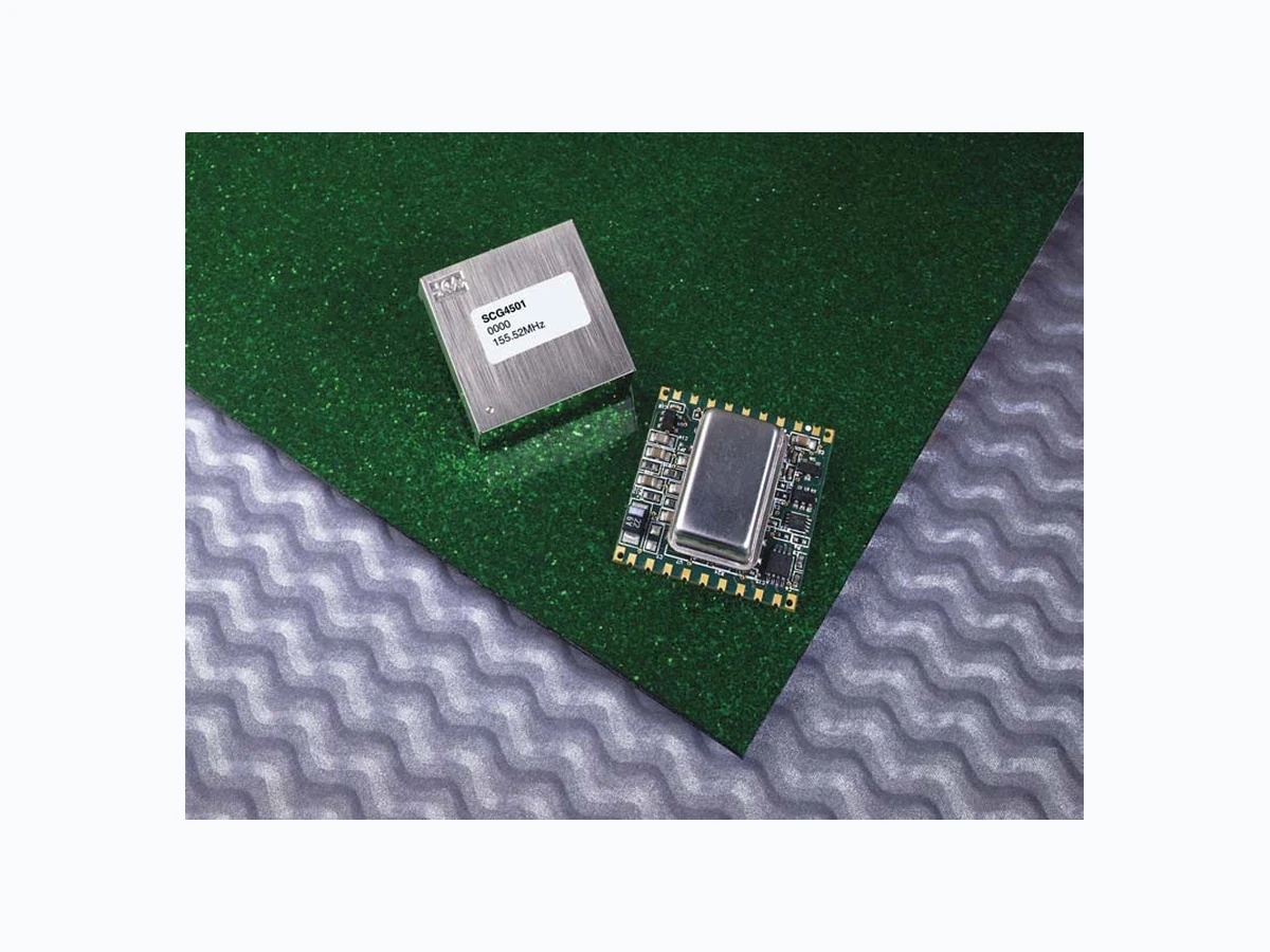
SCG4501 ETC2
Document overview
- Manufacturer or author: pROVIDED bY www.digicamel.com(free datasheet download site)
- PDF pages: 16
Technical content
Features
- ± 32 ppm Capture/Pull-In Range Phase Locked Output Frequency Control Intrinsically Low Jitter Crystal Oscillator LVPECL Outputs with Disable Function Dual Input References LOR & LOL combined alarm output Force Free Run Function Automatic Free Run operation on loss of both References A & B Input Duty Cycle Tolerant 3.3V dc Power Supply Small Size: 1 Square Inch SCG4501 Synchronous Clock Generators PLL
2111 Comprehensive Drive
Aurora, Illinois 60505 Phone: 630-851-4722 Fax: 630-851-5040 www.conwin.com Bulletin SG040 Page 1 of 16 Revision P01 Date 13 NOV 03 Issued By MBatts
Preliminary Data Sheet #: SG040 Page 2 of 16 Rev: P01 Date: 11/13/03 © Copyright 2003 The Connor-Winfield Corp. All Rights Reserved Specifications subject to change without notice Absolute Maximum Rating Table 1 Symbol Parameter Minimum Nominal Maximum Units Notes Vcc Power Supply Voltage -0.5 - +4.0 Volts 1.0 Vi Input Voltage -0.5 - +5.5 Volts 1.0 Ts Storage Temperature -65.0 - +100 °C 1.0 General Description The SCG4501 is a mixed-signal phase locked loop generating LVPECL outputs from an intrinsically low jitter, voltage controlled, crystal oscillator. The LVPECL outputs may be disabled. The SCG4501 can lock to one of two external references, which is selectable using the SEL AB input select pin. The unit has a fast acquisition time of about 1.5 seconds and it is tolerant of different reference duty cycles. The SCG4501 includes an alarm output that indicates deviations from normal operation. If a Loss- of-Reference (LOR) or Loss-of-Lock (LOL) is detected the alarm with indicate the need for a reference rearrangement. If both references A and B are absent the module will enter Free Run operation. The FR status pin will indicate that the module is in Free Run operation. Frequency stability during Free Run operation is guaranteed to ±20 ppm. Additionally the Free Run mode may be entered manually. The package dimensions are 1” x 1.025” x .45” on a 6 layer FR4 board with castellated pins. Parts are assembled using high temperature solder to withstand 63/37 alloys, 180°C surface mount reflow processes. Maximum Dimension Package Outline Figure 1 Block Diagram Figure 2
8 KHz PHASE
Q QN 1 / N ALARM LOW JITTER VCXO FREE RUN STATUS OPTIONAL REFERENCE OUTPUT FORCE FREE RUN ENABLE/ TRI-STATE 33 Ω 10 kΩ 10 kΩ 10 kΩ 10 kΩ 33 Ω 33 Ω DPFD
Preliminary Data Sheet #: SG040 Page 3 of 16 Rev: P01 Date: 11/13/03 © Copyright 2003 The Connor-Winfield Corp. All Rights Reserved Specifications subject to change without notice NOTES: 1.0 Operation of the device at these or any other condition beyond those listed under Operating Specifications is not implied. Exposure to Absolute Maximum Rating conditions for extended periods of time may affect device reliability. 2.0 Requires external regulation and supply decoupling. (22 uF , 330 pF) 3.0 3db loop response. 4.0 50-ohm load biased to 1.3 volts. 5.0 Entry into Free Run doesn’t meet requirement for initial 2.33 seconds of self-timing. 6.0 If the selected reference is removed system response to the ALARM must be less than 10µs. Operating Specifications Table 2 Symbol Parameter Minimum Nominal Maximum Units Notes Vcc Power Supply Voltage 3.135 3.3 3.465 Volts 2.0 Icc Power Supply Current 170 230 280 mA 4.0 To Temperature Range 0 - 70 °C Ffr Free Run Frequency -20 - 20 ppm Fcap Capture/pull-in range -32 - 32 ppm Fbw Jitter Filter Bandwidth - - 10 Hz 3.0 Tjtol Input Jitter Tolerance 31.25 - - µs 8 kHz Ref. units (Input Jitter Frequencies ≥ 10 Hz) 1 - - µs 19.44 MHz Ref. units Taq Typical Acquisition Time Data Acquisition from a cold power-up: Phase lock within 12ns: 50 sec Phase lock settled: 220 sec Alarm time: <1.5 sec Acquisition from Free Run: Phase lock within 12ns: 50 sec Phase lock settled: 220 sec Alarm time: Typically no alarm Frequency lock with a 20PPM reference frequency step: Typically 0.5s. Phase lock during a switch between equal frequency references: Typically 0.5s, no alarm should be issued Trf Output Rise and Fall Time (20% 80%) 100 225 350 ps 4.0 DC Output Duty Cycle 40 50 60 % MTIE sr MTIE at Synchronization Rearrangement GR-253-CORE.1999 R5-136 5.0, 6.0 Dynamic Offset Range (0°- 25°) -50 - 50 ns Dynamic Offset Range (25°- 70°) -50 - 50 ns Output Jitter Specifications Table 3 Jitter BW 10 Hz - 1 MHz SONET Jitter BW 12 kHz - 20 MHz Frequency (MHz) pS (RMS) m UI pS (RMS) m UI
Preliminary Data Sheet #: SG040 Page 4 of 16 Rev: P01 Date: 11/13/03 © Copyright 2003 The Connor-Winfield Corp. All Rights Reserved Specifications subject to change without notice NOTES: A Active FR Free Run Mode NA Not Active RA Locked to Reference A RB Locked to Reference B U Unstable (due to conditions shown, switch to active reference or Free Run) X Don’t care Input And Output Characteristics Table 4 Symbol Parameter Minimum Nominal Maximum Units Notes CMOS Input and Output Characteristics Vih High Level Input Voltage 2.0 - 5.5 V Vil Low Level Input Voltage 0.0 - 0.8 V Tio I/O to Output Valid - - 10 ns C l Output Capacitance - - 10 pF Voh High Level Output Voltage 2.4 - - V Vol Low Level Output Voltage - - 0.4 V Tir Input Reference Pulse Width 12.5 - - ns PECL Output Characteristics Voh High Level PECL Voltage 2.27 2.34 2.52 V Vol Low Level PECL Voltage 1.49 1.51 1.68 V C l Output Capacitance - - 10 pF Tskew Differential Output Skew - 50 - ps Input Selection / Output Response Table 5 INPUTS OUTPUTS NOTE RESET ENABLE SEL AB REF A REF B FR FR status ALARM Q QN 1 0 XXXX 1 X X X F R X 1 XXXX X X 0 1 0 0 XXX1 1 X X X F R 00 0 A A 0 0 0 X X R A 00 1 A A 0 0 0 X X R B 00 0 N A A 0 0 1 X X U 00 1 N A A 0 0 0 X X R B 00 1 A N A 0 0 1 X X U 00 0 A N A 0 0 0 X X R A
00 X N A N A 0 1 1 X X F R
Preliminary Data Sheet #: SG040 Page 6 of 16 Rev: P01 Date: 11/13/03 © Copyright 2003 The Connor-Winfield Corp. All Rights Reserved Specifications subject to change without notice Typical MTIE at Synchronization Rearrangement. Reference B Equal to Inverse of Reference A, No Modulation. Figure 5
Preliminary Data Sheet #: SG040 Page 7 of 16 Rev: P01 Date: 11/13/03 © Copyright 2003 The Connor-Winfield Corp. All Rights Reserved Specifications subject to change without notice Pin Description Table 6 Pin # Pin Name Pin Information Note 1 ENABLE/TRI-STATE VCXO Enable. (Enable = 0, Disable = 1 = CMOS Outputs Tri-stated) 9.0 2 TCK No Connection, Internal Factory Programming Input. 8.0 3 TDO No Connection, Internal Factory Programming Input. 8.0 4 REF A CMOS Reference Frequency Input. 5 SEL AB Input Reference Select Pin. (REFA = 0, REFB = 1) 9.0 6 RESET RESET. (RESET = 1) 9.0 7 REF B CMOS Reference Frequency Input. 8V ee Ground. 9F R status Free Run Status. (FR = 1) 10 V cc Supply Voltage relative to ground. 11 N/C No Connection. (Optional Reference Output Available) 8.0, 8.1 12 ALARM Loss of Reference / Lock alarm. (Alarm = 1) 13 FR Force Free Run. (Phase Lock = 0, Free Run = 1) 9.0 14 TDI No Connection, Internal Factory Programming Input. 8.0 15 TMS No Connection, Internal Factory Programming Input. 8.0 16 QN LVPECL Complementary Output. 17 V ee Ground. 18 Q LVPECL Output. Circuit Board Footprint & Keepout Recommendations Figure 6 0.8400 [21.34 mm] 1.0400 [26.42 mm] 0.8650 [21.97 mm] 0.1000 [2.54 mm] 0.0350 [0.89 mm] 0.0650 [1.65 mm] 0.1000 [2.54 mm] Keep Out Area 1.0700 [27.18 mm] NOTES
8.0 Do not connect pin
8.1 Contact a Sales Representative for availibilty
and use of optional reference output
9.0 Input pulled to ground
Preliminary Data Sheet #: SG040 Page 8 of 16 Rev: P01 Date: 11/13/03 © Copyright 2003 The Connor-Winfield Corp. All Rights Reserved Specifications subject to change without notice LOL (Internal Signal) Phase Detector (Internal Signal) External Reference (Selected Input A or B) Internal Reference (Internal Signal) LOR (Internal Signal) 4 2 2 2 2 2 2 2 2 2 2 2 2 2 2 Start-up Region 1 1 Alarm Output (LOR + LOL) Start-up Region
19.44 MHz Reference Input Units 8 kHz Reference Input Units
< 31.25 µsec 31.25 µsec > 31.25 µsec < 1 µsec > 1 µsec 1 µsec2 4 125 µsec wide rangeLOR is active when LOL is active 5 Minimum pulse width = 2 µsec Minimum pulse width = 62.5 µsec During Start-up, The LOL Alaram will pulse during the few seconds of operation Loss of Reference Condition Alarm Timing Figure 7 AlarmTiming Legend Use for all alarm timing diagrams Table 7
Preliminary Data Sheet #: SG040 Page 9 of 16 Rev: P01 Date: 11/13/03 © Copyright 2003 The Connor-Winfield Corp. All Rights Reserved Specifications subject to change without notice LOL (Internal Signal) Phase Detector (Internal Signal) External Reference (Selected Input A or B) Internal Reference (Internal Signal) LOR (Internal Signal) 3 3 2 2 2 2 2 2 2 2 2 2 1 1 1 1 2 2 2 2 Alarm Output (LOR + LOL) Loss of Lock Condition Alarm Timing Figure 8
Preliminary Data Sheet #: SG040 Page 13 of 16 Rev: P01 Date: 11/13/03 © Copyright 2003 The Connor-Winfield Corp. All Rights Reserved Specifications subject to change without notice Recommended PECL Termination Figure 15 50Ω SCGXXXX LVPECL OUTPUT Q QN Vcc GND 50Ω Transmission Line
3.3 VDC
82Ω 50Ω Transmission Line LVPECL INPUT D DN Vcc GND Q QN Vcc GND LVPECL INPUT D DN Vcc GND 50Ω 130Ω 82Ω D DN Vcc GND 50Ω Transmission Line 50Ω Transmission Line Q QN Vcc GND Vcc - 2 VDC Vcc - 2 VDC 100Ω 50Ω Transmission Line 50Ω Transmission Line 130Ω 150Ω 150Ω If PECL outputs do not drive a long line (< 0.5”), a single 150Ω termination resistor to ground may be used for each pin.
Preliminary Data Sheet #: SG040 Page 14 of 16 Rev: P01 Date: 11/13/03 © Copyright 2003 The Connor-Winfield Corp. All Rights Reserved Specifications subject to change without notice Tape and Reel Packaging Figure 16
Preliminary Data Sheet #: SG040 Page 15 of 16 Rev: P01 Date: 11/13/03 © Copyright 2003 The Connor-Winfield Corp. All Rights Reserved Specifications subject to change without notice Solder Profile Figure 17 Temp 100 150 200 250 12345678 Time(minutes) (C˚) Recommended Reflow Profile Peak Temp:217C˚ MaxRiseSlope:1.5C˚/Sec Time Above150C˚:100Sec Model Comparison Table Table 8 Max Model Input Duty Oscillator Output Notes Ref Freq Cycle (Synchronized Output) SCG4500 8 kHz/8 kHz 40/60 77.76 MHz,155.52 MHz,125 MHz Basic Model SCG4501 8 kHz/8 kHz 40/60 77.76 MHz,155.52 MHz,125 MHz ±32 ppm Pull-in range SCG4510 2@1.544 MHz 40/60 155.52 MHz SCG4520 2@19.44 MHz 40/60 77.76 MHz,155.52 MHz SCG4540 2@10 kHz 40/60 163.84 MHz Other low jitter line card solutions from Connor-Winfield SCG51 Series Single input, jitter filtered with Free Run, 1 CMOS and 3 LVPECL outputs up to 622.08 MHz. SCG102A/104A Single input, frequency selectable, LVPECL clock smoothers from 77.76 to 777.76 MHz. SCG2000 Series Single input, jitter filtered with 20ppm Free Run, CMOS outputs from 8 kHz to 125.0 MHz. SCG2500 Series Dual input, jitter filtered with Free Run, CMOS outputs from 8 kHz to 125.0 MHz. SCG3000 Series Single input, jitter filtered with Dual LVPECL outputs. SCG4000 Series Single input, jitter filtered with 20ppm Free Run, LVPECL outputs from 77.76 MHz to 180 MHz. SCG4600 Series Dual input, jitter filtered with Free Run, 1 CML differential pair output up to 622.08 MHz.
Revision Revision Date Note P00 12/20/01 Preliminary Release P01 11/13/03 Updated to V3.01