
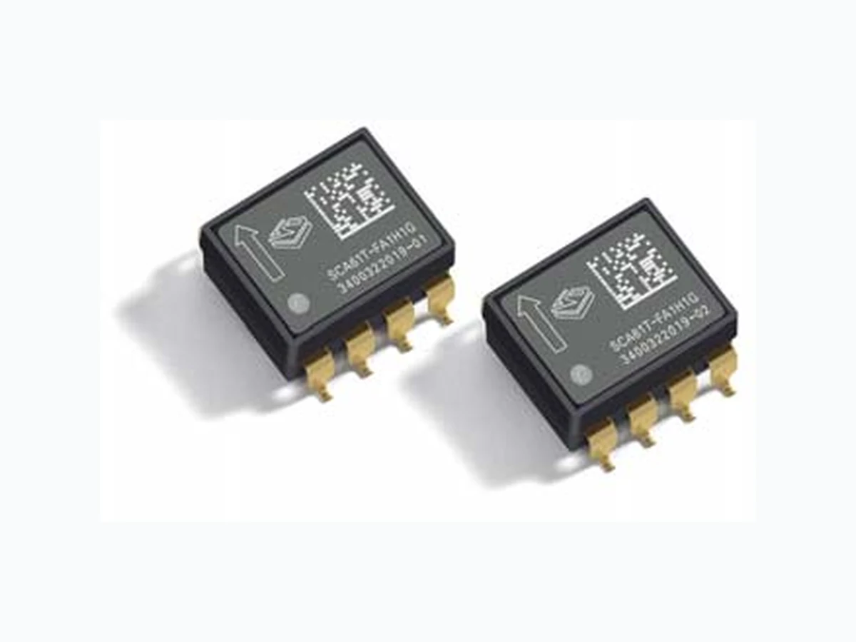
SCA61T ETC2
Document overview
- Manufacturer or author: Provided By www.digicamel.com(FREE DATASHEET DOWNLOAD SITE)
- PDF pages: 18
Technical content
Features
- Measuring ranges ±30° SCA61T-FAHH1G and ± 90° SCA61T-FA1H1G
- 0.0025° resolution (10 Hz BW, analog output)
- Sensing element controlled over damped frequency response (-3dB 18Hz)
- Robust design, high shock durability (20000g)
- Excellent stability over temperature and time
- Single +5 V supply
- Ratiometric analog voltage outputs
- Digital SPI inclination and temperature output
- Comprehensive failure detection features o True self test by deflecting the sensing elements’ proof mass by electrostatic force. o Continuous sensing element interconnection failure check. o Continuous memory parity check.
- RoHS compliant
- Compatible with Pb-free reflow solder process
Applications
- Platform leveling and stabilization
- Leveling instruments
- Acceleration and motion measurement
Figure 1. Functional block diagram
VTI Technologies Oy S ubject to changes 2/18 TABLE OF CONTENTS
VTI Technologies Oy S ubject to changes 3/18
1 Electrical Specifications
The SCA61T product family comprises two versions, the SCA61T-FAHH1G and the SCA61T- FA1H1G, that differ in measurement range. The product version specific performance specifications are listed in the following table bel ow. All other specifications are common to both versions. Vdd=5.00V and ambient temperature unless otherwise specified.
1.1 Absolute Maximum Ratings
Supply voltage (VDD) Voltage at input / output pins Storage temperature Operating temperature Mechanical shock -0.3 V to +5.5V -0.3V to (VDD + 0.3V) -55°C to +125°C -40°C to +125°C Drop from 1 meter on a concrete surface (20000g). Powered or non-powered
1.2 Performance Characteristics
Parameter Condition SCA61T- FAHH1G SCA61T- FA1H1G Units Measuring range Nominal ±30 ±0.5 ±90 ±1.0 g Frequency response –3dB LP (1 8-28 8-28 Hz Offset (Output at 0g) Ratiometric output Vdd/2 Vdd/2 V Offset calibration error ±0.11 ±0.23 ° Offset Digital Output 1024 1024 LSB Sensitivity between 0…1° (2 V/g mV/° Sensitivity calibration error ±0.5 ±0.5 % Sensitivity Digital Output 1638 819 LSB / g -25…85°C (typical) ±0.008 ±0.008 °/°C Offset temperature dependency -40…125°C (max) ±0.86 ±0.86 ° Typical non-linearity Measuring range ±0.11 ±0.57 ° Digital output resolution between 0…1° (2 0.035 0.07 Bits ° / LSB Analog output resolution Bandwidth 10 Hz (3 0.0025 0.0025 ° Cross-axis sensitivity Max. 4 4 % Long term Stability (4 <0.014 <0.014 ° Note 1. The frequency response is determined by the sensing element’s internal gas damping. Note 2. The angle output has SIN curve relationship to voltage output refer to paragraph 2.2 Note 3. Resolution = Noise density * √(bandwidth) Note 4. Power continuously connected (@ 23°C).
VTI Technologies Oy S ubject to changes 4/18
1.3 Electrical Characteristics
Parameter Condition Min. Typ Max. Units Supply voltage Vdd 4.75 5.0 5.25 V Current consumption Vdd = 5 V; No load 2.5 4 mA Operating temperature -40 +125 °C Analog resistive output load Vout to Vdd or GND 10 kOhm Analog capacitive output load Vout to Vdd or GND 20 nF Start-up delay Reset and parity check 10 ms
1.4 SPI Interface DC Characteristics
Parameter Conditions Symbol Min Typ Max Unit
1.4.1.1.1 Input terminal CSB
Pull up current V IN = 0 V I PU 13 22 35 µA Input high voltage VIH 4 Vdd+0.3 V Input low voltage V IL -0.3 1 V Hysteresis VHYST 0.23*Vdd V Input capacitance C IN 2 pF
1.4.1.1.2 Input terminal MOSI, SCK
Pull down current V IN = 5 V I PD 9 17 29 µA Input high voltage VIH 4 Vdd+0.3 V Input low voltage V IL -0.3 1 V Hysteresis VHYST 0.23*Vdd V Input capacitance C IN 2 pF
1.4.1.1.3 Output terminal MISO
Output high voltage I > -1mA V OH Vdd- 0.5 V Output low voltage I < 1 mA VOL 0.5 V Tristate leakage 0 < V MISO < Vdd ILEAK 5 100 pA
1.5 SPI Interface AC Characteristics
Parameter Condition Min. Typ. Max. Units Output load @500kHz 1 nF SPI clock frequency 500 kHz Internal A/D conversion time 150 µs Data transfer time @500kHz 38 µs
1.6 SPI Interface Ti ming Specifications
Figure 2. Timing diagram for SPI communication
1.7 Electrical Connection
Figure 3. SCA61T electrical connection
1 SCK Input Serial clock
2 MISO Output Master in slave out; data output
3 MOSI Input Master out slave in; data input
4 GND Supply Ground
5 CSB Input Chip select (active low)
6 ST Input Self test input
7 Out Output Output
8 VDD Supply Positive supply voltage (+5V DC)
1.8 Typical Performance Characteristics
following diagrams. The 3 sigma limits represents 99.73% of the SCA61T population. Figure 4. Typical temperature dependency of the SCA61T offset
1 SCK
2 MISO
3 MOSI
8 VDD
7 OUT
Figure 5. Typical temperature dependency of SCA61T sensitivity
1.9 Additional External Compensation
2 Functional Description
2.1 Measuring Directions
Figure 8. The measuring direction of the SCA61T
2.2 Voltage to Angle Conversion
with SCA61T-FAHH1G and 2 V/g with SCA61T-FA1H1G. the angle measurement error if straight line conversion is used.
2.3 Ratiometric Output
supply voltage. If the SCA61T supply voltage is fl uctuating, the SCA61T output will also vary.
2.4 SPI Serial Interface
always operates as a slave device in master-slave operation mode. of wires for serial data input (MOSI), serial data output (MISO) and serial clock (SCK). Figure 9. Typical SPI connection The SPI interface in VTI products is designed to support any micro controller that uses an SPI bus.
- commands and data are shifted; MSB first, LSB last
- each output data/status bits are shifted out on the falling edge of SCK (MISO line)
- each bit is sampled on the rising edge of SCK (MOSI line)
- after the device is selected with the falli ng edge of CSB, an 8-bit command is received. The command defines the operations to be performed
- the rising edge of CSB ends all data transfer and resets internal counter and command register
- if an invalid command is received, no data is shifted into the chip and the MISO remains in high impedance state until the falling edge of CSB. This reinitializes the serial communication.
- data transfer to MOSI continues immediately after receiving the command in all cases where data is to be written to SCA61T’s internal registers
- data transfer out from MISO starts with the falli ng edge of SCK immediately after the last bit of the SPI command is sampled in on the rising edge of SCK
- maximum SPI clock frequency is 500kHz
- maximum data transfer speed for RDAX is 5300 samples per sec / channel The SPI command can be either an individual command or a combination of command and data. In the case of combined command and data, the input data follows uninterruptedly the SPI command and the output data is shifted out parallel with the input data. The SPI interface uses an 8-bit instruction (or command) register. The list of commands is given in Table below. Command Name Command Format Description: MEAS 00000000 Measure mode (normal operation mode after power on) RWTR 00001000 Read and write temperature data register RDSR 00001010 Read status register RLOAD 00001011 Reload NV data to memory output register STX 00001110 Activate Self test for X-channel RDAX 00010000 Read X-channel acceleration through SPI Measure mode (MEAS) is standard operation mode after powe r-up. During normal operation, the MEAS command is the exit command from Self test. Read temperature data register (RWTR) reads temperature data register during normal operation without effecting the oper ation. Temperature data register is updated every 150 µs. The load operation is disabled whenever the CSB signal is low, hence CSB must stay high at least 150 µs prior the RWTR command in order to guarantee co rrect data. The data transfer is presented in Figure below. The data is transferred MSB first. In normal operation, it does not matter what data is written into temperature data register during the RWTR command and hence writing all zeros is recommended. 7 6 5 4 3 2 1 0 7 6 5 4 3 2 1 0 CSB SCK MI SO MOSI 0 1 2 3 4 5 6 7 8 9 10 11 12 13 14 15 HIGH I MPEDANCE COMMAND DATA IN DATA OUT
Figure 10. Command and 8 bit temperature data transmission over the SPI stored in acceleration data register X. that is fed out MSB first and LSB last.
Figure 11. Command and 11 bit acceleration data transmission over the SPI
2.5 Digital Output to Angle Conversion
output values with -5, -1 0, 1 and 5 degree tilt angles.
2.6 Self Test and Fa ilure Detection Modes
command on the self test input, or through the SPI.
- Sensing element movement check
- ASIC signal path check
- PCB signal path check
- Micro controller A/D and signal path check The created deflection can be seen in both the SPI and analogue output. The self test function is activated digitally by a STX command, and de-activated by a MEAS command. Self test can be also activated applying logic”1” (positive supply voltage level) to ST pin (pins 6) of SCA61T. The self test Input high voltage level is 4 – Vdd+0.3 V and input low voltage level is 0.3 – 1 V.
Figure 12. Self test wave forms V1 = initial output voltage before the self test function is activated. V2 = output voltage during the self test function. initial value after the specified stabilization time. After a longer time (max. 1 second) V1=V3. T5 = Rise time during self test.
VTI Technologies Oy S ubject to changes 14/18 083.1 197 −= CountsT T1 [ms] T2 [ms] T3 [ms] T4 [ms] T5 [ms] V2: V3: (4.75V @Vdd=5V) 0.95*V1-1.05*V1
2.7 Temperature Measurement
The SCA61T has an internal temperature sensor, which is used for internal offset compensation. The temperature information is also available for additional external compensation. The temperature sensor can be accessed via the SPI interface and the temperature reading is an 8-bit word (0…255). The transfer function is expressed with the following formula: Where: Counts Temperature reading T Temperature in °C The temperature measurement output is not calibrated. The internal temperature compensation routine uses relative results where absolute accuracy is not needed. If the temperature measurement results are used for additional external compensation then one point calibration in the system level is needed to remove the offset. With external one point calibration the accuracy of the temperature measurement is about ±1 °C.
3 Application Information
3.1 Recommended Circuit Diagrams a nd Printed Circuit Board Layouts
both the SCA61T and Analog/Digital converter. Use low pass RC filter with 5.11 kΩ and 10nF on the SCA61T output to minimize clock noise. power supply or GND connection strips on PCB. Figure 13. Analog connection and layout example Figure 14. SPI connection example
3.2 Recommended Printed Ci rcuit Board Footprint
Figure 15. Recommended PCB footprint
4 Mechanical Specifications and Reflow Soldering
4.1 Mechanical Specifica tions (Reference only)
RoHS compliance: RoHS compliant lead free component. Co-planarity error 0.1mm max. Figure 16. Mechanical dimensions of the SCA61T. (Dimensions in mm)
4.2 Reflow Soldering
normal SMD pick-and-place equipment. Figure 17. Recommended SCA61T body temperature profile during reflow soldering. Ref. Average ramp-up rate (TL to TP) 3°C/second max. 3°C/second max.
- Preheating time and temperatures according to solder paste manufacturer.
- It is important that the part is parallel to t he PCB plane and that there is no angular alignment error from intended measuring direction during assembly process.
- Wave soldering is not recommended.
- Ultrasonic cleaning is not allowed. The sensing element may be damaged by ultrasonic cleaning process.
VTI Technologies Oy S ubject to changes 18/18
5 Document Change Control
Version Date Change Description A 1.9.-06 Initial release
6 Contact Information
(head office) VTI Technologies Oy P.O. Box 27 Myllynkivenkuja 6 FI-01621 Vantaa Finland Tel. +358 9 879 181 Fax +358 9 8791 8791 E-mail: sales@vti.fi Germany VTI Technologies Oy Branch Office Frankfurt Rennbahnstrasse 72-74 D-60528 Frankfurt am Main, Germany Tel. +49 69 6786 880 Fax +49 69 6786 8829 E-mail: sales.de@vti.fi USA VTI Technologies, Inc. One Park Lane Blvd. Suite 804 - East Tower Dearborn, MI 48126 USA Tel. +1 313 425 0850 Fax +1 313 425 0860 E-mail sales@vtitechnologies.com Japan VTI Technologies Oy Tokyo Office Tokyo-to, Minato-ku 2-7-16 Bureau Toranomon 401105-0001 Japan Tel. +81 3 6277 6618 Fax +81 3 6277 6619 China VTI Technologies Shanghai Office 6th floor, Room 618
780 Cailun Lu
201203 Shanghai
P.R. China Tel. +86 21 5132 0418 or +86 21 5132 0400 *112 Fax +86 21 513 20 416 E-mail: forename.surname@vti.fi To find out your local sales representative visit www.vti.fi VTI Technologies reserves all rights to modify this document without prior notice.