
S9012 LEIDITECH
Document overview
- Manufacturer or author: Provided By www.digicamel.com(FREE DATASHEET DOWNLOAD SITE)
- PDF pages: 4
Technical content
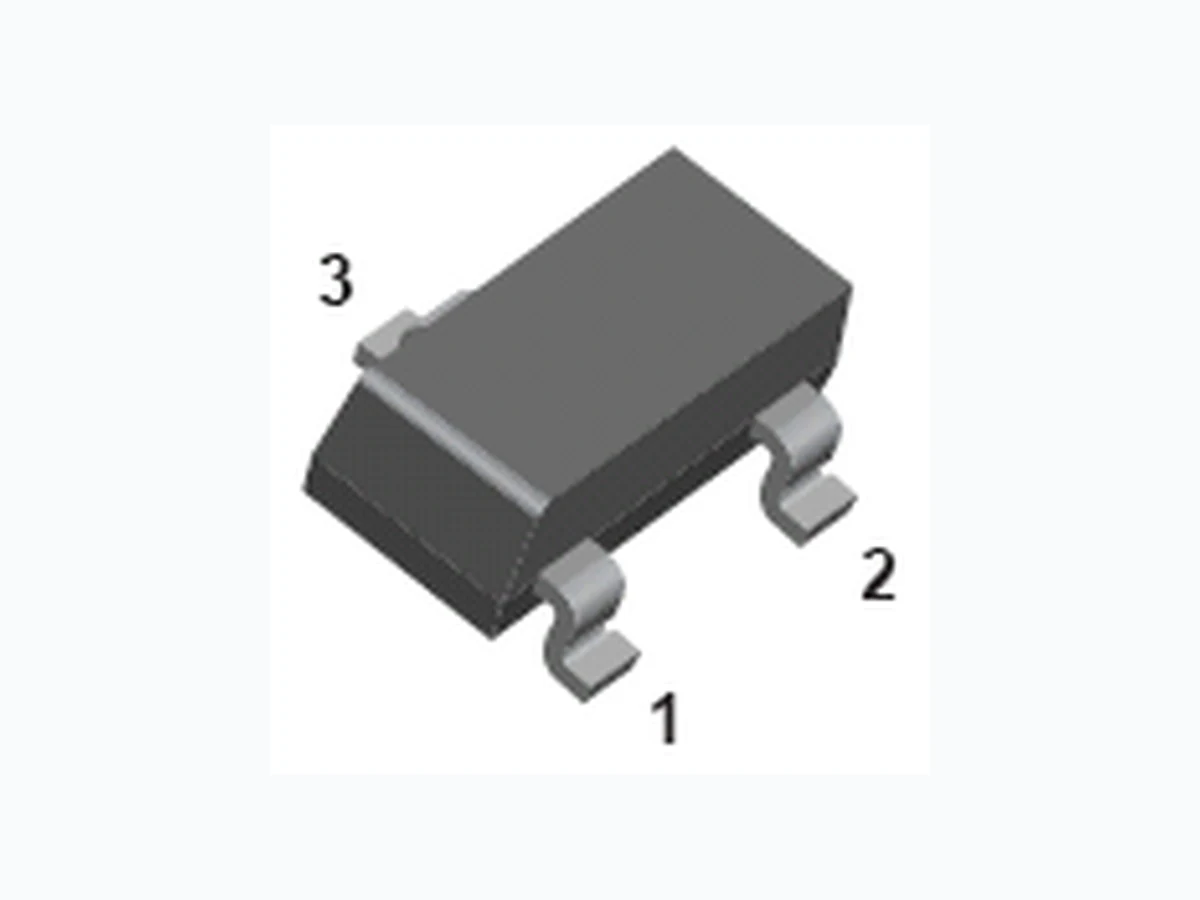
Rev : www.leiditech.com01.08.2021 1/4 S9 0 12 PNP Silicon Epitax ial Planar Transistor FEAT URES z High Collector Curr ent.(IC= -500mA) z Complementary To S9013. z Excellent HFE Linearity. APPLICAT IONS z H i g h C o l l e c t o r C u r r e n t . SOT-23 ORDERING INFORMAT ION Type No. Marking Package Code Shipping S9012 2T1 SOT-23 3000/Tape&Reel MAXIMUM RATING @ Ta =25℃ unless otherwise specified Symbol Parameter Value Units VCBO Collector-Bas e Voltage -40 V VCEO Collector-Emitter Voltage -25 V VEBO Emitter-Base Voltage -5 V IC Collector Curr ent -Continuous -500 mA PC Collector Dissipation 300 mW Tj,Tstg Junction and Storage Temperature -55~1 50 ℃ Pb Lead-free PA CKAGE INFORMATION
: www.leiditech.com 2/4 ELECTRICAL CHARACTERISTICS @ T a=25℃ unless otherwise specified Parameter Symbol Test conditions MIN TYP MAX UNIT Collector-ba se breakdown voltage V(BR)CBO IC=-100μA,IE=0 -40 V Collector-em itter breakdown voltage V(BR)CEO I C=-1mA,IB=0 -25 V Emitter-base breakdow n voltage V (BR)EBO I E=-100μA,IC=0 -5 V Collector cut-off current ICBO VCB=-40V ,IE=0 -0.1 μA Collector cut-off current ICEO VCE=-20V ,IB=0 -0.1 μA Emitter cut-off current IEBO VEB=-5V ,IC=0 -0.1 μA DC c urrent gain hFE VCE=-1V ,IC=-50mA 120 400 Collector-em itter saturation voltage VCE(sa t) IC=-500mA, IB= -50mA -0.6 V Base-emitter saturation voltage VBE(sat) IC=-500mA, IB= -50mA -1.2 V Transition frequency fT VCE=-6V, IC= -20mA f=30MHz 150 MHz Collector output capacitance Cob VCB=-10V,IE=0,f=1MHz 5 pF CLASSIFICA TION OF h FE(1) Rank L H J Rang e 120-200 200-350 300-400 MARKING 2T1 01.08.2021 S9 0 12
: www.leiditech.com 3/4 TYPICAL CHARACTERISTICS @ T a=25℃ unless otherwise specified 01.08.2021 S9 0 12
nghai Leiditech Electronic Co.,Ltd Email: sale1@leiditech.com Tel : +86- 021 50828806 Fax : +86- 021 50477059 Rev : www.leiditech.com 4/4 P ACKAGE OUTLINE Plastic surface mounted package SOT-23 SOLDERING FOOTPRINT U n i t : m m SOT -23 Dim Min Max A 2.85 2.95 B 1.25 1.35 C 1.0T ypical D 0.37 0.43 E 0.35 0.48 G 1.85 1.95 H 0.02 0.1 J 0.1T ypical K 2.35 2.45 All Dimensio ns in mm 01.08.2021 S9 0 12