

 Download PDF
S8650 HAMAMATSU
Document overview
- PDF pages: 2
Technical content
Page 1
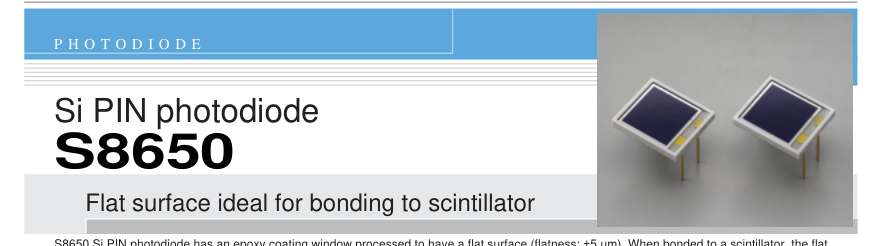
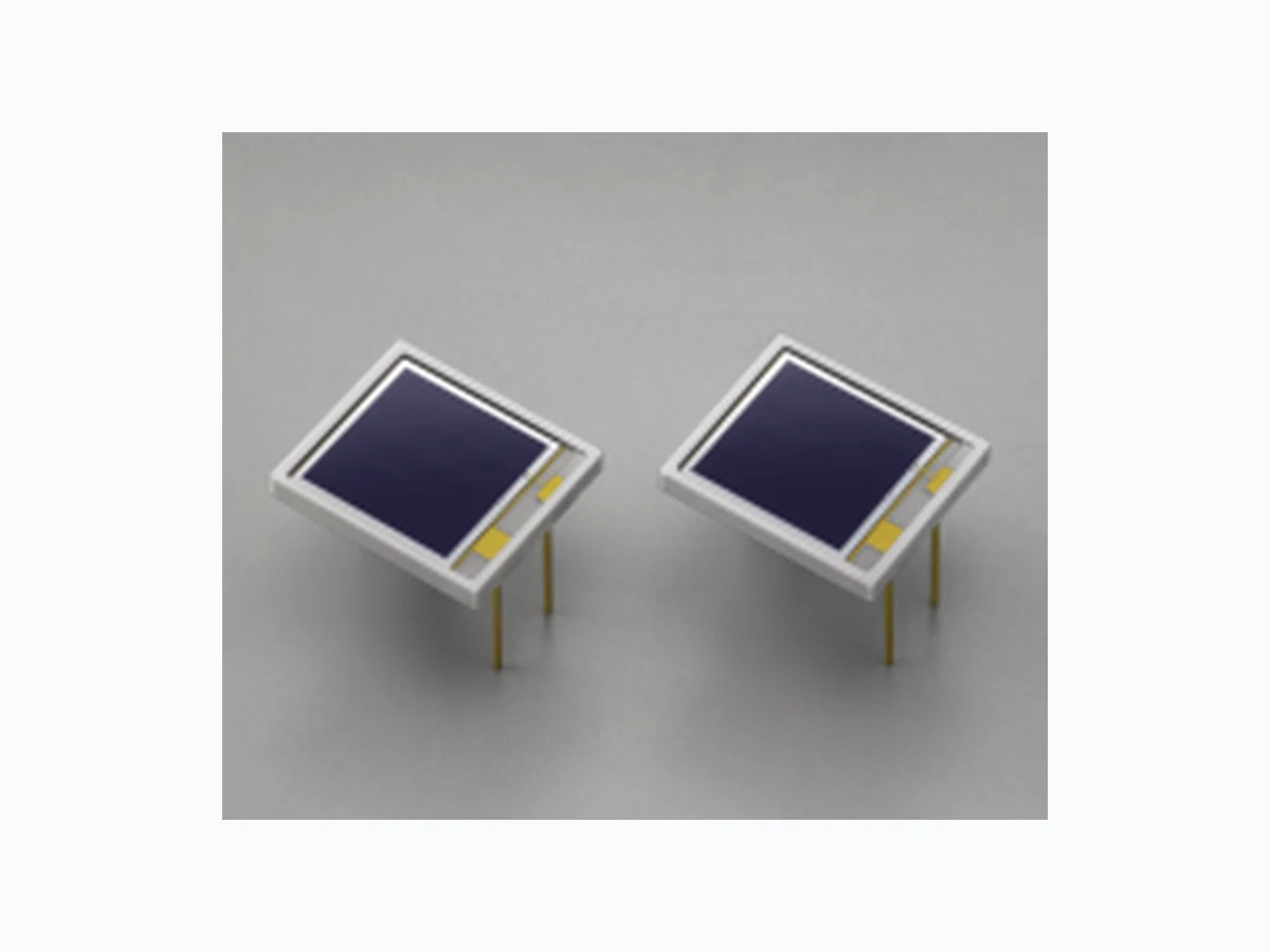
S8650 Si PIN photodiode has an epoxy coating window processed to have a flat surface (flatness: ±5 µm). When bonded to a scintillator, the flat surface allows highly tight coupling to the scintillator so bubbles are unlikely to penetrate in between. We also accept special orders for machining flat surfaces on other ceramic package products. Feel free to place an order with us.

(Other sizes are also available on request.)
I Absolute maximum ratings (Ta=25 °C)
| Parameter | Symbol | Value | Unit |
|---|---|---|---|
| Reverse voltage | VR Max. | 100 | V |
| Operating temperature | Topr | -20 to +60 | °C |
| Storage temperature | Tstg | -20 to +80 | °C |
I Electrical and optical characteristics (Ta=25 °C)
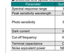
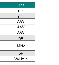
| Symbol | Condition | Min. | Typ. | Max. |
|---|---|---|---|---|
| λ | - | 320 to 1100 | - | |
| λp | - | 960 | - | |
| S | λ=λp | - | 0.66 | - |
| BGO: λ=480 nm | - | 0.30 | - | |
| CsI (Tl): λ=540 nm | - | 0.37 | - | |
| ID | VR=70 V | - | 2 | 6 |
| fc | λ=780 nm, VR=70 V RL=50 Ω, -3 dB | - | 40 | - |
| Ct | VR=70 V, f=1 MHz | - | 40 | - |
| NEP | VR=70 V, λ=λp | 3.8 × 10⁻¹⁴ | - |

Page 2
Si PIN photodiode S8650
I Spectral response
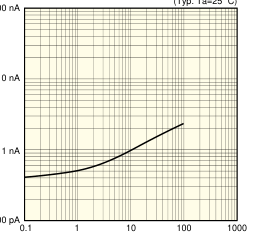
I Dark current vs. reverse voltage
(Typ. Ta=25 ˚C)
(Typ. Ta=25 ˚C)
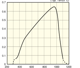
WAVELENGTH (nm)
REVERSE VOLTAGE (V)
KPINB0254EA
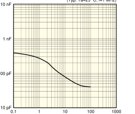
I Terminal capacitance vs. reverse voltage
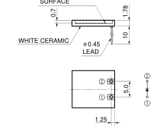
I Dimensional outline (unit: mm)
+0
(Typ. Ta=25 ˚C, f=1 MHz)
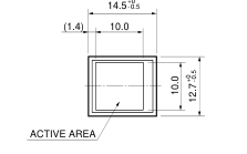
PHOTOSENSITIVE SURFACE
REVERSE VOLTAGE (V)
KPINB00256EA
KPINB00255EA
Epoxy resin flatness: ±5 µm Tolerance unless otherwise noted: ±0.2
KPINA0088EA
Information furnished by HAMAMATSU is believed to be reliable. However, no responsibility is assumed for possible inaccuracies or omissions. Specifications are subject to change without notice. No patent rights are granted to any of the circuits described herein. ©2006 Hamamatsu Photonics K.K.
HAMAMATSU PHOTONICS K.K., Solid State Division
1126-1 Ichino-cho, Higashi-ku, Hamamatsu City, 435-8558 Japan, Telephone: (81) 53-434-3311, Fax: (81) 53-434-5184, www.hamamatsu.com U.S.A.: Hamamatsu Corporation: 360 Foothill Road, P.O.Box 6910, Bridgewater, N.J. 08807-0910, U.S.A., Telephone: (1) 908-231-0960, Fax: (1) 908-231-1218 Germany: Hamamatsu Photonics Deutschland GmbH: Arzbergerstr. 10, D-82211 Herrsching am Ammersee, Germany, Telephone: (49) 08152-3750, Fax: (49) 08152-2658 France: Hamamatsu Photonics France S.A.R.L.: 19, Rue du Saule Trapu, Parc du Moulin de Massy, 91882 Massy Cedex, France, Telephone: 33-(1) 69 53 71 00, Fax: 33-(1) 69 53 71 10 United Kingdom: Hamamatsu Photonics UK Limited: 2 Howard Court, 10 Tewin Road, Welwyn Garden City, Hertfordshire AL7 1BW, United Kingdom, Telephone: (44) 1707-294888, Fax: (44) 1707-325777
North Europe: Hamamatsu Photonics Norden AB: Smidesvägen 12, SE-171 41 Solna, Sweden, Telephone: (46) 8-509-031-00, Fax: (46) 8-509-031-01 Italy: Hamamatsu Photonics Italia S.R.L.: Strada della Moia, 1/E, 20020 Arese, (Milano), Italy, Telephone: (39) 02-935-81-733, Fax: (39) 02-935-81-741