Download PDF
S6503P KODENSHI
Document overview
- PDF pages: 14
Technical content
Page 1
Power Factor Collector
Description
It is Adaptable to a Discontinuous Mode of Operation that the S6503/P is Advanced PFC (Power Factor Correction) Controller for the High Density Switching Mode Power Supply and Electronic Ballast systems. The Bulky External components are eliminated in the Internal Start-up circuits, though it is taken in Independent Boost Converter Operation. What is more, instead of the External components, the Low Pass Filter is mounted in Internal Current Sense block. Internal Clamping of the Error Amplifier and Multiplier Output improve turn on Overshoot Characteristics and Current Limiting. The One of features is able to prevent Abnormal Condition, Open Lamp & Over Voltage.
Features
- Very Precise Adjustable Output OVP (Dynamic & Static OVP Function)
- Extremely Low Start-Up Current
- Low Operating Supply Current
- Internal Start-Up Timer
- Power Factor Maximizer & THD Minimizer Circuit
- Complete Wide Range Operation
- Feedback Open Protection
- Minimum On Timer
- Current Sense Filter On Chip
- Disable Function
- Extremely Minimized External Part Counts High Speed Response Time
Applications
- Switching Mode Power Supply (SMPS)
- Electronic Ballast
Ordering Information
Type NO.
Marking
Package Code
S6503
S6503
SOP-8
S6503P
S6503
DIP - 8
Page 2
Block Diagram
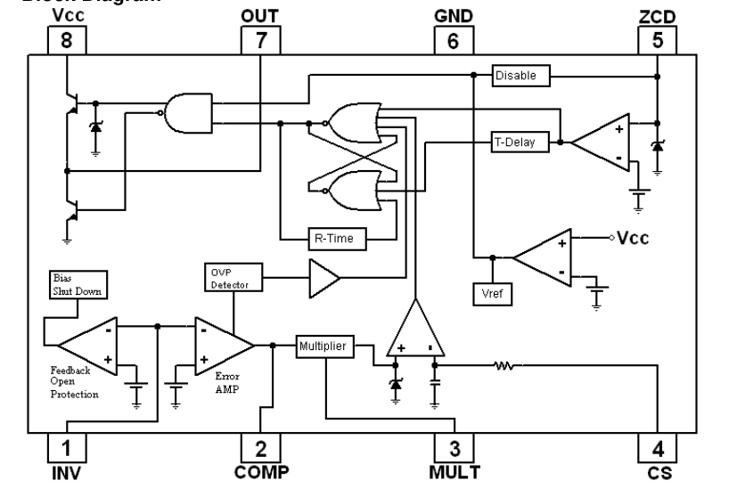
Pin Description
| No | Symbol | I/O | Description |
|---|---|---|---|
| 1 | INV | I | Inverting Input of Error Amplifier |
| 2 | COMP | O | Output of Error Amplifier |
| 3 | MULT | I | Multiplier Input |
| 4 | CS | I | Current Sense Input |
| 5 | ZCD | I | Zero Current Detect |
| 6 | GND | - | Ground |
| 7 | OUT | O | Totem-Pole Output |
| 8 | VCC | - | Power Supply Voltage |
Page 3
Absolute Maximum Ratings
| Characteristics | Symbol | Value | Unit | |
|---|---|---|---|---|
| Maximum Supply Voltage | V CCMAX | 27 | V | |
| Output Peak Current | I PEAK | ±500 | ㎃ | |
| Analog Input & Output (Pin 1,2,3,4,5) | V INMAX | -0.3 ~ 7 | V | |
| ZCD Input Maximum Current | I ZCD | ±10 | ㎃ | |
| Power Dissipation | P DMAX | SOP-8 | 600 | ㎽ |
| DIP-8 | 800 | |||
| Operating Junction Temperature | T j | -35 ~ 150 | ℃ | |
| Storage Temperature | T stg | -55 ~ 150 | ℃ | |
Electrical Characteristics
(Ta = -25℃ to 125℃, VCC=14V unless otherwise specified.)
| Characteristics | Symbol | Test Condition | Min. | Typ. | Max. | Unit |
|---|---|---|---|---|---|---|
| Supply Voltage & Current Section | ||||||
| V Turn-On Threshold CC | V CC(On) | V Increasing CC | 11 | 12 | 13 | V |
| V Turn-Off Threshold CC | V CC(Off) | V Decreasing CC | 8.7 | 9.5 | 10.3 | V |
| Hysteresis Voltage | HYS | 2 | 2.5 | 3 | V | |
| Start-Up Current | I ST | Before Turn-On | 20 | 40 | 70 | ㎂ |
| Quiescent Current | I Q | No Switching | 1 | 4 | 6 | ㎃ |
| Operating Supply Current | I CC | C =1nF, f =50KHz L sw | 2 | 5 | 8 | ㎃ |
| Operating Current at OVP | I CC_OVP | V =2.7V INV | 0.5 | 2 | 4 | ㎃ |
| Operating Current at Disable | I CC_DIS | V <150mV ZCD | 0.5 | 2 | 4 | ㎃ |
| Error Amplifier Section | ||||||
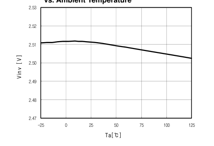
| Input Voltage | V INV | Ta=25℃ | 2.465 | 2.5 | 2.535 | V |
| Line Regulation | dV INV | V =12 ~27V CC | - | 0.1 | 5 | ㎷ |
| Input Bias Current | I INV | -0.5 | -0.1 | 0.5 | ㎂ | |
| Open Loop Gain | Av | 60 | 80 | - | ㏈ | |
| Gain Bandwidth | GB | - | 1 | - | ㎒ | |
| Output Source Current | I SOURCE | V =4V,V =2.4V COMP INV | -2 | -4 | - | ㎃ |
| Output Sink Current | I SINK | V =4V,V =2.6V COMP INV | 3 | 5 | - | ㎃ |
| Upper Clamp Voltage | V UPPER | I =-100uA,V =2.4V O INV | - | 5.6 | - | V |
| Lower Clamp Voltage | V LOWER | I =100uA, V =2.6V O INV | - | 2.25 | - | V |
| Feedback Open Protection Threshold Voltage | V fo | V Decreasing INV | 150 | 200 | 250 | ㎷ |
Page 4
Electrical Characteristics (Continued)
(Ta = -25℃ to 125℃, VCC=14V unless otherwise specified.)
| Characteristics | Symbol | Test Condition | Min. | Typ. | Max. | Unit |
|---|---|---|---|---|---|---|
| Multiplier Section | ||||||
| Linear Operating Voltage | VMULT | 2.8 | 3.2 | - | V | |
| Output Maximum Slope | dV /dV CS MULT | V = 0.5 ~ 0.9V, MULT V = Upper Clamp COMP | 1.3 | 1.5 | 1.7 | V/V |
| Mltiplier Gain | K | Ta=25℃, V =1V MULT V =3.5V COMP | 0.5 | 0.65 | 0.75 | 1/V |
| Current Sense (CS) Section | ||||||
| Reference Clamp Voltage | V CS | V =2.5V, MULT V =Upper Clamp COMP | 1.65 | 1.75 | 1.85 | V |
| Input Bias Current | I CS | V = 0 ~ 1.6V CS | -0.5 | -0.1 | 0.5 | ㎂ |
| Delay to Output | T d(H-L) | - | 200 | - | ㎱ | |
| Zero Current Detector (ZCD) Section | ||||||
| Input Threshold Voltage | V ZCD | V Increasing ZCD | 1.8 | 2.1 | 2.4 | V |
| Hysteresis Voltage | HY(ZCD) | - | 0.5 | - | V | |
| Upper Clamp Voltage | V ) CLAMP(H | I = 3mA ZCD | 48 | 5.4 | 6 | V |
| Lower Clamp Voltage | V ) CLAMP(L | I = -3mA ZCD | 0.3 | 0.6 | - | V |
| Input Bias Current | I ZCD | V = 1 ~ 3V ZCD | - | 1 | - | ㎂ |
| Source Current | I SOURCE(ZCD) | -3 | - | - | ㎃ | |
| Sink Current | I SINK(ZCD) | 3 | - | - | ㎃ | |
| Disable Input Voltage | V DIS | V Decreasing ZCD | 150 | 200 | 250 | ㎷ |
| Reset Current after Disable | I DIS | Pin5 = 0V | -30 | -80 | - | ㎂ |
| Restart Timer Section | ||||||
| Restart Time Delay | t rst | 70 | 130 | 300 | ㎲ | |
Page 5
Electrical Characteristics (Continued)
(Ta = -25℃ to 125℃, Vcc=14V unless otherwise specified.)
| Characteristics | Symbol | Test Condition | Min. | Typ. | Max. | Unit |
|---|---|---|---|---|---|---|
| Output Section | ||||||
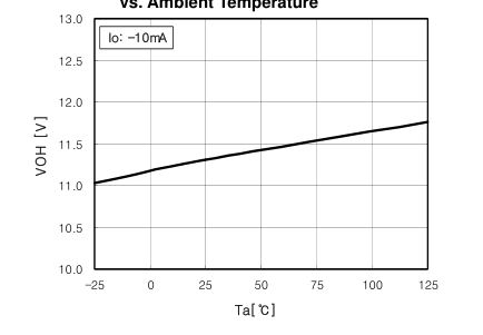
| Output High Voltage | V OH | I =-10mA O | 10.5 | 11.5 | 12.5 | V |
| I =-100mA O | 10 | 11 | 12 | V | ||
| Maximum Voltage | V OMAX | V =20V, I =-1mA CC o | 11 | 13 | 15 | V |
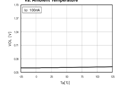
| Output Low Voltage | V OL | I =10mA O | - | 0.1 | 1 | V |
| I =100mA O | - | 1.2 | 2.5 | V | ||
| Output Voltage with UVLO Activated | V O(UV) | I =1mA O | - | - | 1 | V |
| Minimum On Time | T ON(MIN) | - | 150 | 1 | ㎱ | |
| Output Rising Time | t r | C = 1nF L | - | 50 | - | ㎱ |
| Output Falling Time | t f | C = 1nF L | - | 50 | - | ㎱ |
| Over Voltage Protector (OVP) Section | ||||||
| Dynamic OVP Current | I OVP | 35 | 40 | 45 | ㎂ | |
| Dynamic OVP Current Hysteresis | I OVP(HYS) | - | 30 | - | ㎂ | |
| Static OVP Threshold Voltage | V OVP | V = 2.7V INV | 2.1 | 2.25 | 2.4 | V |
Page 6
Application Information
- Main Inductor
2
×( V −V )×V /(4
V × P × f )
L =η
O P P O O
Where,
η: Efficiency (0.95)
VO: DC Link Voltage VP: Input Peak Voltage PO: Output Power f: Switching Frequency
- Resistor for Current Sense RS = 1.75/ILP Where, ILP: Inductor Peak Current
- Resistor for Multiplier RML<0.69 x RMU / (VP– 0.69) Where, RMU: Under Resistor for Multiplier Input RML: Lower Resistor for Multiplier Input
- Resistor for Error Amplifier REL = 2.5 x REU / (VO – 2.5) Where, REU: Under Resistor for Error Amplifier Inverting Input REL: Lower Resistor for Error Amplifier Inverting Input
Page 7
- Over Voltage Protector (OVP) △VO = REU[Ω ] x 40[㎂]
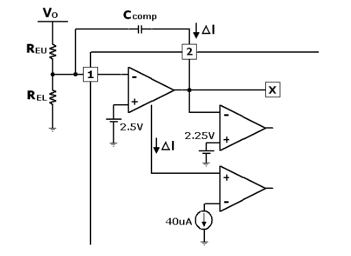
Fig.1 Over Voltage Protection Circuit
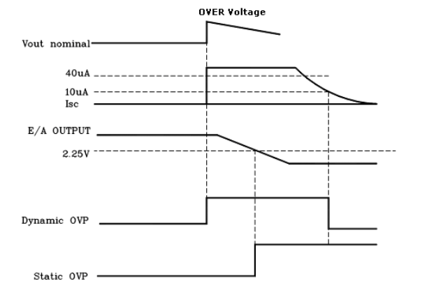
Fig.2 OVP Operating Timing Chart
Page 8
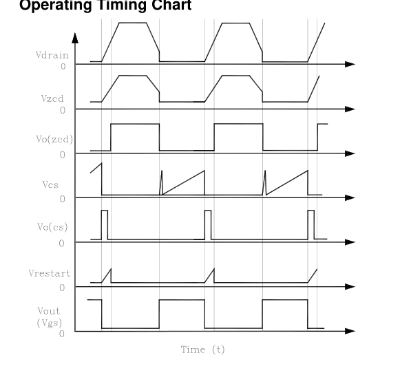
Operating Timing Chart
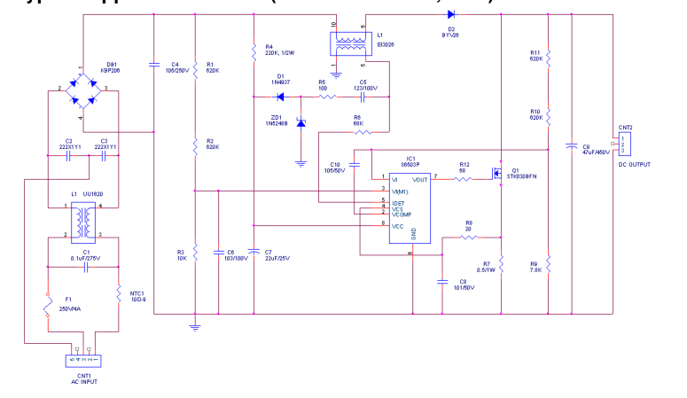
Typical Application Circuit (85VAC ~ 265VAC, 80W)
Page 9
Electrical Characteristic Curves
Fig.1 Operating Supply Current vs. Supply Voltage
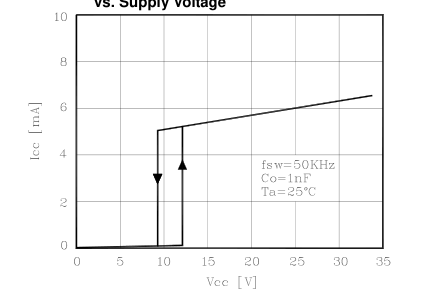
Fig.3 Output Voltage
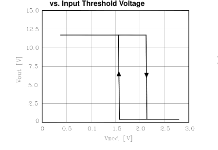
Fig. 5 Output Voltage vs. Input Voltage
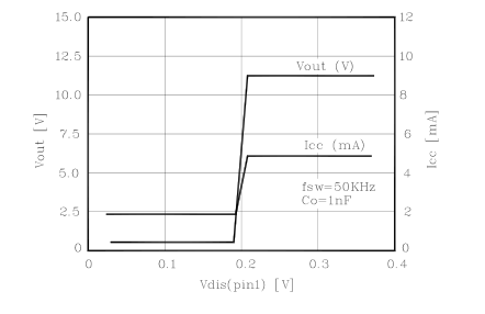
Fig.2 Start-Up Current vs. Supply Voltage
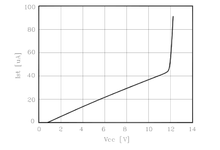
Fig.4 Output Voltage
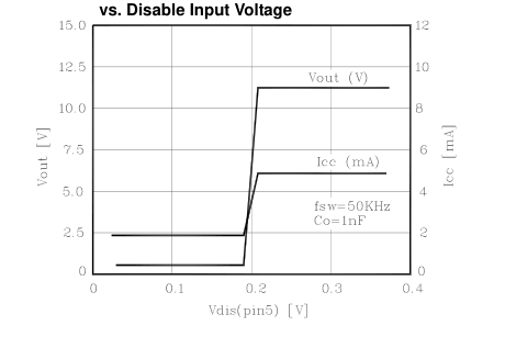
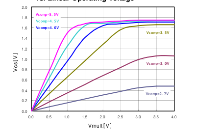
Fig.6 Reference Clamp Voltage vs. Linear Operating Voltage
Page 10
Fig.8 Output Low Voltage
Fig.7 Output High Voltage
vs. Output Sink Current
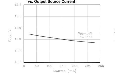
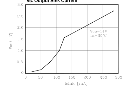
Fig.10 Multiplier Gain vs.
Fig.9 Operating Supply Voltage
Ambient Temperature
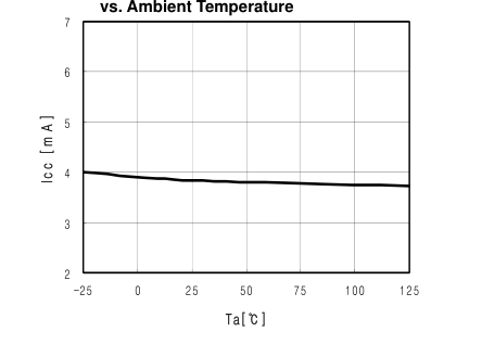
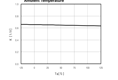
Fig.12 Output Low Voltage
Fig.11 Output High Voltage
vs. Ambient Temperature
vs. Ambient Temperature
Page 11
Fig.13 Output Maximum Slop vs. Ambient Temperature
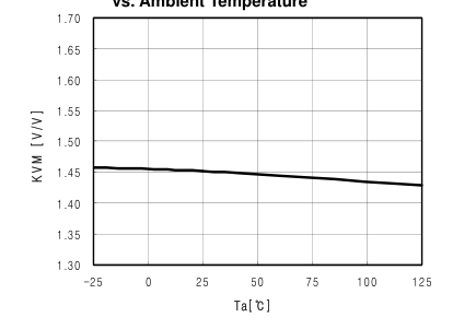
Fig.14 Input Voltage vs. Ambient Temperature
Page 12
Outline Dimension (Unit : mm)
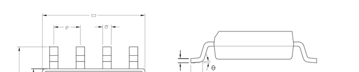
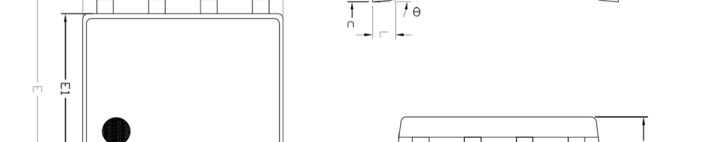
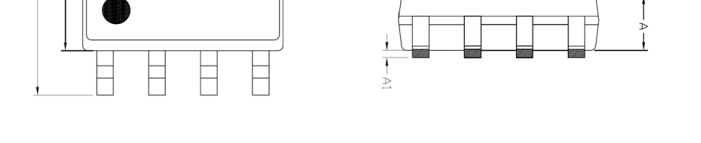


※ Recommend PCB solder land (Unit : mm)
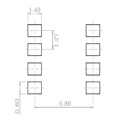
Page 13
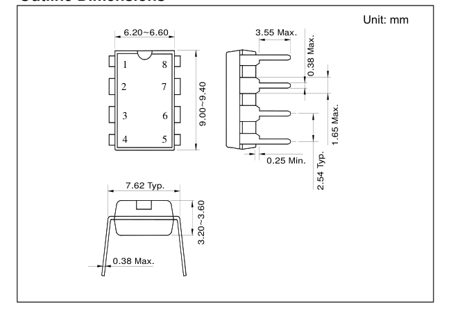
Outline Dimensions
Page 14