
S2F VISHAY
Document overview
- Manufacturer or author: Provided By www.digicamel.com(FREE DATASHEET DOWNLOAD SITE)
- PDF pages: 8
Technical content
www.vishay.com Vishay Sfernice Revision: 09-Oct-2025 1 Document Number: 50087 For technical questions, contact: sferthinfilm@vishay.com THIS DOCUMENT IS SUBJECT TO CHANGE WITHOUT NOTICE. THE PRODUCTS DESCRIBED HEREIN AND THIS DOCUMENT ARE SUBJECT TO SPECIFIC DISCLAIMERS, SET FORTH AT www.vishay.com/doc?91000 Fast Acting Thin Film Chip Fuses LINKS TO ADDITIONAL RESOURCES
FEATURES
- 3 sizes: 0402, 0603, and 1206
- Maximal protection as fuses are designed to open in t < 1 min at 200 % overload
- UL 248-14 compliant
- From 0.315 A to 7 A
- Low resistance
- Body temperature rising < 75 °C at 100 % rated current
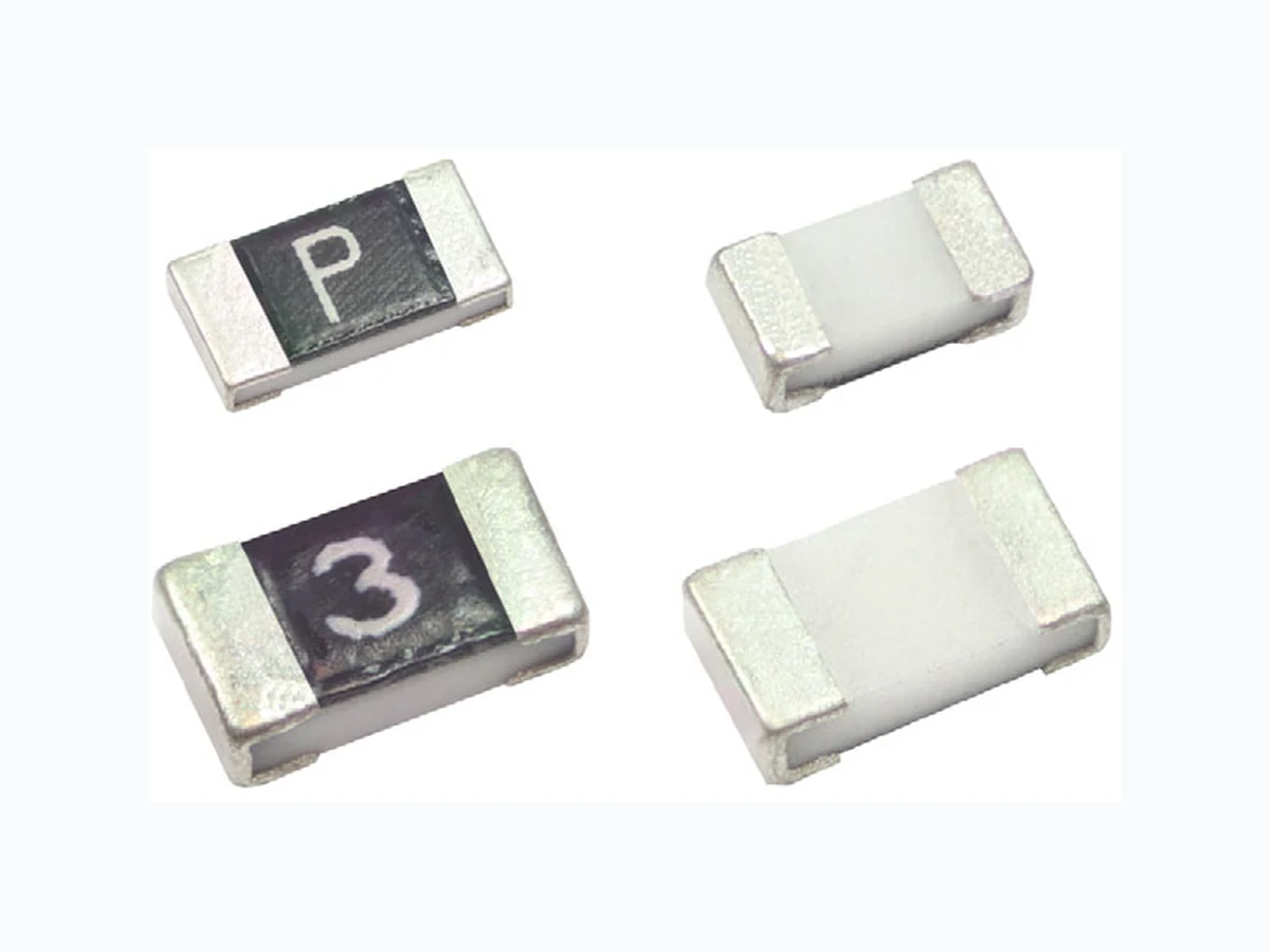
- Material categorization: fo r definitions of compliance please see www.vishay.com/doc?99912 S2F thin film chip fuses are designed to ensure circuit continuity with minimal resistance and reliable interruption under overload condition. Particularly adapted to be co mpatible with numerous applications in th e sector of electronics. They comply with industrial and government standa rds, as well as Vishay quality and reliabil ity requirements. For very fast acting see S3F datasheet. DIMENSIONS 333DDD3 D 3D Models TECHNICAL SPECIFICATIONS DESCRIPTION S2F0402 S2F0603 S2F1206 Imperial size 0402 0603 1206 Rated current I Rated voltage Umax. DC 32 V 32 V and 50 V 32 V and 63 V Cold resistance at I ≤ 0.1 x IN 12 mΩ to 690 mΩ 11 mΩ to 496 mΩ 7.5 mΩ to 517 mΩ Fusing time Open within 1 min at 200 % rated power Body temperature rise < 75 °C at 100 % rated current Operating temperature range -25 °C to 125 °C with proper derating factor Approved UL 248-14 recognition file E548286 DIMENSIONS AND TOLERANCES in millimeters (inches) TYPE A B C D E S2F0402 1.00 ± 0.10 (0.039 ± 0.004) 0.52 ± 0.05 (0.020 ± 0.002) 0.35 ± 0.05 (0.014 ± 0.002) 0.20 ± 0.10 (0.008 ± 0.004) 0.25 ± 0.10 (0.010 ± 0.004) S2F0603 1.60 ± 0.10 (0.063 ± 0.004) 0.80 ± 0.10 (0.031 ± 0.004) 0.45 ± 0.10 (0.018 ± 0.004) 0.30 ± 0.20 (0.012 ± 0.008) 0.35 ± 0.20 (0.014 ± 0.008) S2F1206 3.10 ± 0.10 (0.122 ± 0.004) 1.55 ± 0.10 (0.061 ± 0.004) 0.60 ± 0.10 (0.024 ± 0.004) 0.50 ± 0.30 (0.020 ± 0.012) 0.50 ± 0.20 (0.020 ± 0.008) A DD C EE B F
www.vishay.com Vishay Sfernice Revision: 09-Oct-2025 2 Document Number: 50087 For technical questions, contact: sferthinfilm@vishay.com THIS DOCUMENT IS SUBJECT TO CHANGE WITHOUT NOTICE. THE PRODUCTS DESCRIBED HEREIN AND THIS DOCUMENT ARE SUBJECT TO SPECIFIC DISCLAIMERS, SET FORTH AT www.vishay.com/doc?91000 LAND PATTERN DIMENSIONS Note (1) Resistance value was measured with less than 10 % of rated current MECHANICAL SPECIFICATIONS Substrate Ceramic Technology Thin film Termination Cu / Ni plating SUGGESTED LAND PATTERN DIMENSIONS in millimeters (inches) TYPE a b c S2F0402 0.55 to 065 (0.022 to 0.026) 1.40 to 1.60 (0.055 to 0.063) 0.74 to 0.94 (0.029 to 0.037) S2F0603 0.85 to 0.95 (0.033 to 0.037) 2.00 to 2.20 (0.079 to 0.087) 1.50 to 1.70 (0.059 to 0.067) S2F1206 0.95 to 1.05 (0.037 to 0.041) 4.40 to 5.00 (0.173 to 0.197) 2.30 to 2.50 (0.091 to 0.098) S2F0402 RATING PART DESIGNATION MARKING RATED CURRENT (A) FUSING TIME RESISTANCE (1) (mΩ), TOLERANCE: ± 25 % RATED VOLTAGE (VDC) BREAKING CAPACITY S2F040232VA315TT D 0.315 Open within 1 min at 200 % rated current 690 32 32 V DC, 35 A S2F040232VA500TT F 0.500 340 S2F040232VA750TT V 0.750 140 S2F040232VA800TT K 0.800 100 S2F040232V1A00TT L 1.000 95 S2F040232V1A25TT M 1.250 57 S2F040232V1A50TT P 1.500 45 S2F040232V1A60TT N 1.600 44 S2F040232V2A00TT S 2.000 33 S2F040232V2A50TT T 2.500 25 S2F040232V3A00TT 3 3.000 19 S2F040232V3A15TT U 3.150 18 S2F040232V4A00TT W 4.000 12 a b c
www.vishay.com Vishay Sfernice Revision: 09-Oct-2025 3 Document Number: 50087 For technical questions, contact: sferthinfilm@vishay.com THIS DOCUMENT IS SUBJECT TO CHANGE WITHOUT NOTICE. THE PRODUCTS DESCRIBED HEREIN AND THIS DOCUMENT ARE SUBJECT TO SPECIFIC DISCLAIMERS, SET FORTH AT www.vishay.com/doc?91000 Note (1) Resistance value was measured with less than 10 % of rated current TEMPERATURE DERATING Normal ambient temperature: 25 °C Operating temperature range: -25 °C to 125 °C, with proper derating factor as below: Chip Fuse Temperature S2F0603 RATING PART DESIGNATION MARKING RATED CURRENT (A) FUSING TIME RESISTANCE (1) (mΩ), TOLERANCE: ± 25 % RATED VOLTAGE (VDC) BREAKING CAPACITY S2F060350VA400TT E 0.40 Open within 1 min at 200 % rated current 496 50 50 V DC, 50 AS2F060350VA500TT F 0.50 290 S2F060332VA630TT I 0.63 205 32 32 V DC, 50 A S2F060332VA800TT K 0.80 132 S2F060332V1A00TT L 1.00 84 S2F060332V1A25TT M 1.25 63 S2F060332V1A50TT P 1.50 50.5 S2F060332V1A60TT N 1.60 45 S2F060332V2A00TT S 2.00 34 S2F060332V2A50TT T 2.50 24.5 S2F060332V3A00TT 3 3.00 20 S2F060332V3A15TT U 3.15 19 S2F060332V4A00TT W 4.00 13 S2F060332V5A00TT Y 5.00 11 S2F1206 RATING PART DESIGNATION MARKING RATED CURRENT (A) FUSING TIME RESISTANCE (1) (mΩ), TOLERANCE: ± 25 % RATED VOLTAGE (VDC) BREAKING CAPACITY S2F120663VA500TT F 0.50 Open within 1 min at 200 % rated current 517 63 63 V DC, 50 A S2F120663VA800TT K 0.80 211 S2F120663V1A00TT L 1.00 132 S2F120663V1A25TT M 1.25 95 S2F120663V1A50TT P 1.50 76 S2F120663V2A00TT S 2.00 40.5 S2F120632V2A50TT T 2.50 31.5 32 32 V DC, 50 A S2F120632V3A00TT 3 3.00 23.25 S2F120632V4A00TT W 4.00 16 S2F120632V5A00TT Y 5.00 12 S2F120632V7A00TT Z 7.00 7.5 100 1000 10000 100 110 120 -25 0 25 50 75 100 125 150 Axis Title 1st line 2nd line 2nd line Percentage of Rating (%) Ambient Temperature (°C)
www.vishay.com Vishay Sfernice Revision: 09-Oct-2025 4 Document Number: 50087 For technical questions, contact: sferthinfilm@vishay.com THIS DOCUMENT IS SUBJECT TO CHANGE WITHOUT NOTICE. THE PRODUCTS DESCRIBED HEREIN AND THIS DOCUMENT ARE SUBJECT TO SPECIFIC DISCLAIMERS, SET FORTH AT www.vishay.com/doc?91000 Note
- Packaging is compliant to EIA-481 Re v. D (IEC 60286, part 3) standard SOLDERING / MOUNTING PARAMETERS Please see the application note ( www.vishay.com/doc?52029). The recommended reflow so lder process parameters are displayed in pages 4 and 5. PERFORMANCES TESTS CONDITIONS REQUIREMENTS PERMISSIBLE CHANGES Carrying capacity Rated current, 4 h No fusing Fusing time 200 % of its rated current Within 5 s Interrupting ability After the fuse is interrupted, rated voltage applied for 30 s again No mechanical damages Bending test Distance between holding points: 90 mm Bending: 3 mm, 1 time, 30 s No mechanical damages Resistance to solder heat 260 °C ± 5 °C, 10 s ± 1 s ± 20 % Solderability 235 °C ± 5 °C, 2 s ± 0.5 s 245 °C ± 5 °C, 2 s ± 0.5 s (lead (Pb)-free) 95 % coverage minimum Temperature rise 100 % of its rated current, measurement of surface temperature < 75 °C Resistance to dry heat 105 °C ± 5 °C, 1000 h ± 20 % Resistance to solvent 23 °C ± 5 °C in isopropyl alcohol, 90 s No evident damages on protective coating and marking Residual resistance DC measurement after fusing 10 k Ω and more Thermal shock -25 °C / 25 °C / 125 °C / 25 °C, 10 cycles PACKAGING SIZE MOQ TAPE WIDTH TAPE PITCH PACKAGING DIMENSIONS 0402 10 000 8 mm 2 mm Ø 180 mm / 7" 0603 5000 4 mm Ø 180 mm / 7" 1206 5000 4 mm Ø 180 mm / 7" GLOBAL PART NUMBER INFORMATION Part Number: S2F060332V1A50TT MODEL SIZE RATING VOLTAGE RATING CURRENT TERMINATION PACKAGING S2F 0402 (1005) 0603 (1608) 1206 (3216) 32V 50V 63V A400 = 0.4 A 1A50 = 1.5 A 3A15 = 3.15 A T = Sn T (tape and reel) = paper tape (5000 / 10 000) ΔR 2F060332S V1 TA 5 0 T
www.vishay.com Vishay Sfernice Revision: 09-Oct-2025 5 Document Number: 50087 For technical questions, contact: sferthinfilm@vishay.com THIS DOCUMENT IS SUBJECT TO CHANGE WITHOUT NOTICE. THE PRODUCTS DESCRIBED HEREIN AND THIS DOCUMENT ARE SUBJECT TO SPECIFIC DISCLAIMERS, SET FORTH AT www.vishay.com/doc?91000 FUNCTIONAL PERFORMANCE S2F04 (0402 Size) Chip Fuse I-t Curve S2F04 (0402 Size) Chip Fuse t-I2t Curve S2F06 (0603 Size) Chip Fuse I-t Curve 100 1000 10000 0.001 0.01 0.1 100 0.1 1 10 100 Axis Title 1st line 2nd line 2nd line Clearing Time (s) Current (A) ▬▬▬ 0.315 A ▬▬▬ 0.500 A ▬▬▬ 0.750 A ▬▬▬ 0.800 A ▬▬▬ 1.000 A ▬▬▬ 1.250 A ▬▬▬ 1.500 A ▬▬▬ 1.600 A ▬▬▬ 2.000 A ▬▬▬ 2.500 A ▬▬▬ 3.000 A ▬▬▬ 3.150 A ▬▬▬ 4.000 A 100 1000 10000 0.001 0.01 0.1 100 0.001 0.01 0.1 1 Axis Title 1st line 2nd line 2nd line Joule Integral (A2s) Clearing Time (s) ▬▬▬ 0.315 A ▬▬▬ 0.500 A ▬▬▬ 0.750 A ▬▬▬ 0.800 A ▬▬▬ 1.000 A ▬▬▬ 1.250 A ▬▬▬ 1.500 A ▬▬▬ 1.600 A ▬▬▬ 2.000 A ▬▬▬ 2.500 A ▬▬▬ 3.000 A ▬▬▬ 3.150 A ▬▬▬ 4.000 A 100 1000 10000 0.001 0.01 0.1 100 0.1 1 10 100 Axis Title 1st line 2nd line 2nd line Clearing Time (s) Current (A) ▬▬▬ 0.400 A ▬▬▬ 0.500 A ▬▬▬ 0.630 A ▬▬▬ 0.800 A ▬▬▬ 1.000 A ▬▬▬ 1.250 A ▬▬▬ 1.500 A ▬▬▬ 1.600 A ▬▬▬ 2.000 A ▬▬▬ 2.500 A ▬▬▬ 3.000 A ▬▬▬ 3.150 A ▬▬▬ 4.000 A ▬▬▬ 5.000 A
www.vishay.com Vishay Sfernice Revision: 09-Oct-2025 6 Document Number: 50087 For technical questions, contact: sferthinfilm@vishay.com THIS DOCUMENT IS SUBJECT TO CHANGE WITHOUT NOTICE. THE PRODUCTS DESCRIBED HEREIN AND THIS DOCUMENT ARE SUBJECT TO SPECIFIC DISCLAIMERS, SET FORTH AT www.vishay.com/doc?91000 S2F06 (0603 Size) Chip Fuse t-I2t Curve S2F12 (1206 Size) Chip Fuse I-t Curve S2F12 (1206 Size) Chip Fuse t-I2t Curve 100 1000 10000 0.001 0.01 0.1 100 0.001 0.01 0.1 1 Axis Title 1st line 2nd line 2nd line Joule Integral (A2s) Clearing Time (s) ▬▬▬ 1.600 A ▬▬▬ 2.000 A ▬▬▬ 2.500 A ▬▬▬ 3.000 A ▬▬▬ 3.150 A ▬▬▬ 4.000 A ▬▬▬ 5.000 A ▬▬▬ 0.400 A ▬▬▬ 0.500 A ▬▬▬ 0.630 A ▬▬▬ 0.800 A ▬▬▬ 1.000 A ▬▬▬ 1.250 A ▬▬▬ 1.500 A 100 1000 10000 0.001 0.01 0.1 100 0.1 1 10 100 Axis Title 1st line 2nd line 2nd line Clearing Time (s) Current (A) ▬▬▬ 0.500 A ▬▬▬ 0.800 A ▬▬▬ 1.000 A ▬▬▬ 1.250 A ▬▬▬ 1.500 A ▬▬▬ 2.000 A ▬▬▬ 2.500 A ▬▬▬ 3.000 A ▬▬▬ 4.000 A ▬▬▬ 5.000 A ▬▬▬ 7.000 A 100 1000 10000 0.001 0.01 0.1 100 0.001 0.01 0.1 1 Axis Title 1st line 2nd line 2nd line Joule Integral (A2s) Clearing Time (s) ▬▬▬ 2.500 A ▬▬▬ 3.000 A ▬▬▬ 4.000 A ▬▬▬ 5.000 A ▬▬▬ 7.000 A ▬▬▬ 0.500 A ▬▬▬ 0.800 A ▬▬▬ 1.000 A ▬▬▬ 1.250 A ▬▬▬ 1.500 A ▬▬▬ 2.000 A
www.vishay.com Vishay Sfernice Revision: 09-Oct-2025 7 Document Number: 50087 For technical questions, contact: sferthinfilm@vishay.com THIS DOCUMENT IS SUBJECT TO CHANGE WITHOUT NOTICE. THE PRODUCTS DESCRIBED HEREIN AND THIS DOCUMENT ARE SUBJECT TO SPECIFIC DISCLAIMERS, SET FORTH AT www.vishay.com/doc?91000 Typical Joule integral values , measured at 10 time s rated current, are displayed in the following table: Furthermore, for repeated numbers of inrush current, another specific derating must be applied: Chip Fuse Clearing by Repeated Rush Current S2F FUSE I2t (A2s) PART NUMBER TYPICAL I2t (A2s) PART NUMBER TYPICAL I2t (A2s) PART NUMBER TYPICAL I2t (A2s) S2F040232VA315TT 0.00203 S2F060350VA400TT 0.004 S2F120663VA500TT 0.011 S2F040232VA500TT 0.00317 S2F060350VA500TT 0.005 S2F120663VA800TT 0.031 S2F040232VA750TT 0.00402 S2F060332VA630TT 0.007 S2F120663V1A00TT 0.034 S2F040232VA800TT 0.00532 S2F060332VA800TT 0.014 S2F120663V1A25TT 0.062 S2F040232V1A00TT 0.00724 S2F060332V1A00TT 0.016 S2F120663V1A50TT 0.144 S2F040232V1A25TT 0.01344 S2F060332V1A25TT 0.027 S2F120663V2A00TT 0.181 S2F040232V1A50TT 0.01356 S2F060332V1A50TT 0.037 S2F120632V2A50TT 0.351 S2F040232V1A60TT 0.01672 S2F060332V1A60TT 0.041 S2F120632V3A00TT 0.501 S2F040232V2A00TT 0.01983 S2F060332V2A00TT 0.044 S2F120632V4A00TT 0.954 S2F040232V2A50TT 0.03763 S2F060332V2A50TT 0.055 S2F120632V5A00TT 0.966 S2F040232V3A00TT 0.05427 S2F060332V3A00TT 0.082 S2F120632V7A00TT 3.250 S2F040232V3A15TT 0.06304 S2F060332V3A15TT 0.089 S2F040232V4A00TT 0.08960 S2F060332V4A00TT 0.239 S2F060332V5A00TT 0.433 i2 .dtt = 0 t () 100 1000 10 000 100 10 100 1000 10 000 100 000 Axis Title 1st line 2nd line 2nd line Ratio of I2t (%) Ratio of I2t Repeat Numbers to Blowing
www.vishay.com Vishay Revision: 01-Jan-2026 1 Document Number: 91000 THIS DOCUMENT IS SUBJECT TO CHANGE WITHOUT NOTICE. THE PRODUCTS DESCRIBED HEREIN AND THIS DOCUMENT ARE SUBJECT TO SPECIFIC DISCLAIMERS, SET FORTH AT www.vishay.com/doc?91000 Disclaimer ALL PRODUCT, PRODUCT SPECIFICATIONS AND DATA AR E SUBJECT TO CHANGE WITH OUT NOTICE TO IMPROVE RELIABILITY, FUNCTION OR DESIGN OR OTHERWISE. Vishay Intertechnology, Inc., its affiliates, agents, and employee s, and all persons acting on it s or their behalf (collectivel y, “Vishay”), disclaim any and all liability for any errors, inaccuracies or incompleteness contained in any datasheet or in any other disclosure relating to any product. Vishay makes no warranty, representation or guarantee regarding the suitability of the products for any particular purpose or the continuing production of any product. To the maximum extent permitted by applicable law, Vishay disclaims (i) any and all liability arising out of the application or use of any product , (ii) any and all liability, including without limitation specia l, consequential or incidental damages, and (iii) any and all implied warranties, incl uding warranties of fitness for particular purpose, non-infringement and merchantability. Statements regarding the suitability of pro ducts for certain types of applications are based on Vishay's knowledge of typical requirements that are often placed on Vishay products in ge neric applications. Such statements are not binding statements about the suitability of products for a particular application. It is the customer's responsibility to validate that a particular product with the properties described in the product specification is suitable for use in a particular application. Parameters provided in datasheets and / or specificat ions may vary in different applications and performance may vary over time. All operating parameters, including typical parameters, must be validated for each customer application by the customer's technical experts. Product specifications do not expand or otherwise modify Vishay's terms and conditions of purchase, including but not limited to the warranty expressed therein. Hyperlinks included in this datasheet may direct users to third-party websites. These links are provided as a convenience and for informational purposes only. Inclusion of these hyperlinks does not constitute an endorsement or an approval by Vishay of any of the products, services or opinions of the corporation, organization or individual associated with the third-party website. Vishay disclaims any and all liability and bears no responsibility for the accuracy, legality or content of the third-party web site or for that of subsequent links. Vishay products are not designed for use in life-saving or life -sustaining applications or any application in which the failure of the Vishay product could result in personal injury or death unless specifically qualified in writing by Vishay. Customers using or selling Vishay products not expressly indicated for use in such applications do so at their own risk. Please contact authorized Vishay personnel to obtain written terms and conditions regarding products designed for such applications. No license, express or implied, by estoppel or otherwise, to any intellectual property rights is granted by this document or by any conduct of Vishay. Product names and markings noted herein may be trademarks of their respective owners. © 2026 VISHAY INTERTECHNOLOGY, INC. ALL RIGHTS RESERVED