
PSD6407 ETC
Document overview
- Manufacturer or author: Provided By www.digicamel.com(FREE DATASHEET DOWNLOAD SITE)
- PDF pages: 16
Technical content
PSD(POSITION SENSITIVE DETECTOR ) SOLID STATEDIVISION
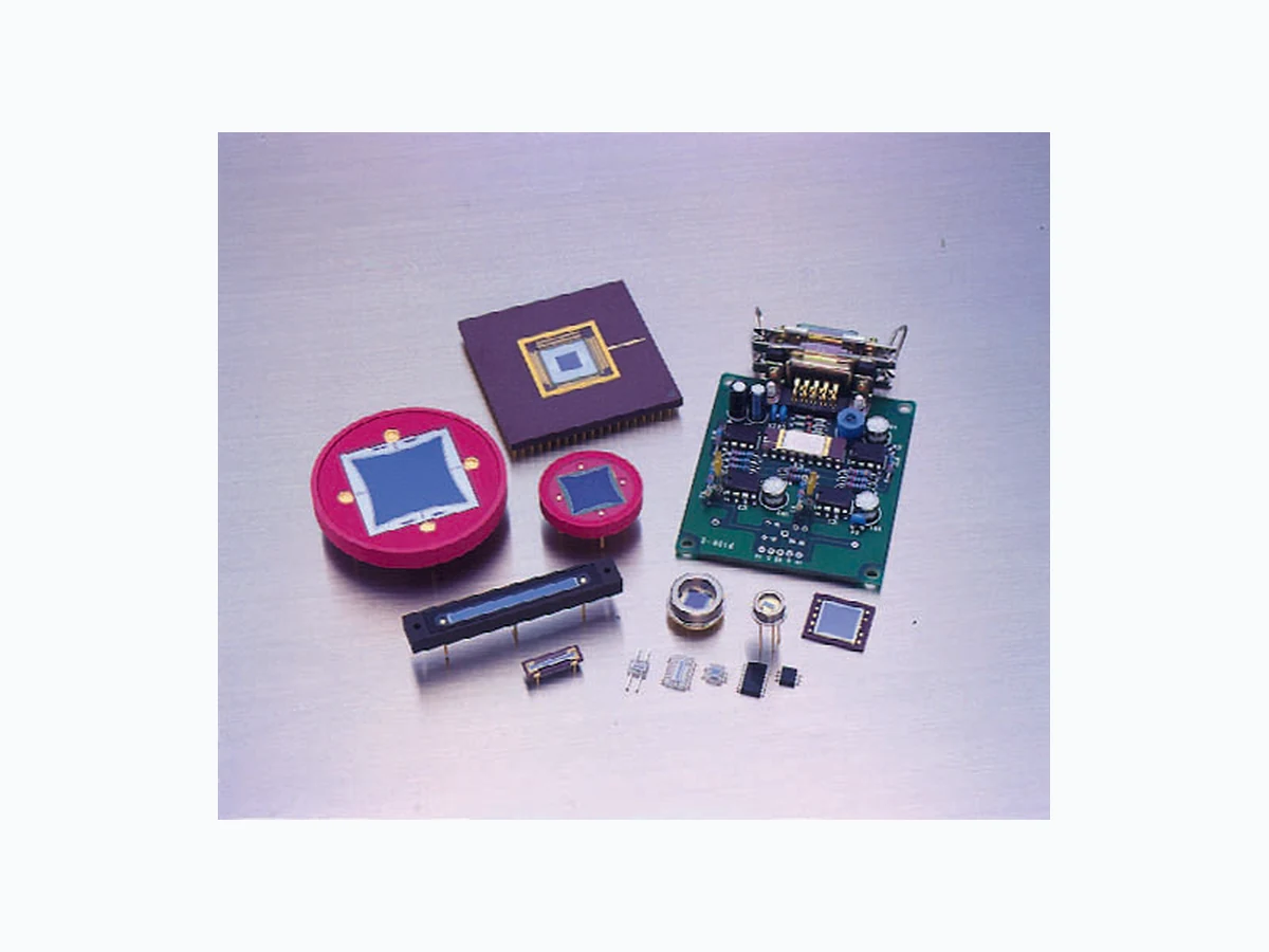
Various methods are available for detecting the position of incident light. These include methods using small discrete detector arrays or multi-element sensors such as CCD sensors. In contrast to these sensors, PSDs (Position Sensitive Detectors) are comprised of a monolithic detector with no discrete elements and provide continuous position data by making use of the surface resistance of the photodiode. PSDs offer advantages such as high position resolution, high-speed response and reliability. What is PSD?
- Excellent position resolution
- Wide spectral response range
- High-speed response
- Detects center-of-gravity position of spot light
- Simultaneously detects light intensity and center-of-gravity position of spot light
- High reliability /K6E Features of PSD
- Position and angle sensing
- Distortion and vibration measurements
- Lens reflection and refraction measurements
- Laser displacement sensing
- Optical remote control
- Optical range finders
- Optical switches
- Camera auto focusing /K6E Applications of PSD
- Basic Principle 2. One-dimensional PSD 3. Two-dimensional PSD 4. Position detection error 5. Position resolution 6. Response speed 7. Saturation photocurrent
CONTENTS
Hamamatsu provides various types of one-dimensional PSDs designed for high-precision distance measurement such as displacement meters, camera auto focusing and optical switches. Our product line includes a visible-cut type for near infrared detection, a red sensitivity enhanced type for red light detection, a microscopic spot light (LD beam, etc.) detection type, and a long, narrow type with an active area exceeding 30 mm. Selection guide PSD (Position Sensitive Detector) is an optoelectronic position sensor utiliz- ing photodiode surface resistance. Unlike discrete element detectors such as CCD, PSD provides continuous position data (X or Y coordinate data) and features high position resolution and high-speed response. 1312 (mm) (mm) (kΩ ) (nm) S6407 1 × 1 1 200 760 to 1100 S6515 1 × 1.2 1.2 140 760 to 1100 S4580-04 760 to 1100 S4580-06 0.8 × 1.5 1.5 140 320 to 1100 S4581-04 760 to 1060 320 to 1060 760 to 1060 760 to 1100 320 to 1100 760 to 1100 760 to 1100 320 to 1100 760 to 1100 440 to 1100 400 to 1100 760 to 1100 320 to 1100 760 to 1100 760 to 1100 320 to 1100 760 to 1100 760 to 1100 320 to 1100 760 to 1100 320 to 1100 320 to 1100 320 to 1100 320 to 1100 700 to 1100 S4581-06 140 S3271-05 1 × 22 400 S4582-04 S4582-06 140 S3272-05 1 × 2.5 2.5 400 S4583-04 S4583-06 140 S3273-05 400 S7879 S8361 * 1 × 33 110 S4584-04 S4584-06 140 S3274-05 1 × 3.5 3.5 400 S7105-04 S7105-06 140 S7105-05 1 × 4.2 4.2 400 S5629 S5629-01 50 S5629-02 1 × 66 300 Plastic S3979 1 × 3 3 140 TO-5 S3931 1 × 6 6 50 S3932 1 × 12 12 50 S1352 2.5 × 34 34 20 S3270 1 × 37 37 15 Ceramic * High sensitivity in the red region type Works with microscopic spot light detection. 1 2 3 4 5 7 8 9 106 Interelectrode resistance Vb=0.1 V Type No. Active area Resistance length Package Spectral response range
S5681 is a 128-element PSD linear array. By scanning a slit-form light beam right and left based on the slit light projection method, S5681 allows measuring a 3-D shape of the object. Two-dimensional PSDs are classified by structure into a tetra-lateral type and a duo-lateral type. The tetra-lateral type features high-speed response and low dark current. The duo-lateral type offers small position detection error and high position resolution. A pin-cushion type, which is a tetra-lateral type with improved active area and electrodes, has a position detection error as small as the duo-lateral type while still having the advantages of the tetra-lateral type. Selection guide (Typ.) Interelectrode resistance Vb=0.1 V (kΩ ) Resistance length (mm) Type No. Package Spectral response range (nm) S5681 Ceramic Active area (mm) 0.025 × 6.375/ 128 elements 1006.375 (Typ.) Interelectrode resistance Vb=0.1 V (kΩ ) S7848 S7848-01 Plastic2 × 2 2 × 2 10 × 10 4.5 × 4.5 5.7 × 5.7 26 × 26 14 × 14 13 × 13S1200 100 Tetra-lateral type Tetra-lateral type S1300 Ceramic13 × 13 Duo-lateral type S2044 Metal4.7 × 4.7 S1880 12 × 12 10 S1881 Ceramic22 × 22 Pin-cushion type (improved tetra-lateral type) Pin-cushion type (improved tetra-lateral type) Pin-cushion type (improved tetra-lateral type) S5990-01 4 × 4 S5991-01 Ceramic chip carrier9 × 9 Type No. PackageStructureActive area (mm) Resistance length (mm) Spectral response range (nm) 3 5 8 9 /K6E Examples of position detectability (Ta=25 ˚C, λ=890 nm, spot light size: φ200 µm) /K6C S1200 KPSDC0017EA /K6C S1300 KPSDC0015EA /K6C S1880 KPSDC0020EA /K6C S5991-01 KPSDC0065EA /K6C S7848 KPSDC0084EA LINE INTERVAL: 1 mm LINE INTERVAL: 1 mm LINE INTERVAL: 1 mm LINE INTERVAL: 1 mm LINE INTERVAL: 0.2 mm Works with microscopic spot light detection 320 to 1060 320 to 1100 320 to 1060 320 to 1060 320 to 1100 760 to 1100 320 to 1100 320 to 1100
PSD signal processing circuit /K6C No complicated adjustments required Position measurements can be made by just connecting to a PSD and power supply (±15 V). /K6C The position (mm) of a spot light from the PSD center is obtained as an output voltage (V). (except C3683-01) /K6C Stable position detection Accurate position data can be detected independent of incident light intensity. /K6C Compact size Head amplifiers, signal addition/subtraction circuits, and analog divider are mounted on a compact PC board. Designed specifically for DC light detection. Designed specifically for pulse (AC) signal detection. Has a synchronous circuit, S/H (sample & hold) circuit and LED driver circuit. Use of a pulse-driven LED ensures reliable operation even under background light. Type No. PSD type Dimensional outline (mm) C3683-01 1-D PSD 66 × 56 × 15 C4674 Pin-cushion type 2-D PSD 90 × 65 × 15 C4757 Duo-lateral type 2-D PSD 92 × 70 × 15 C4758 Tetra-lateral type 2-D PSD 90 × 65 × 15 Type No. * Can not be modulated. PSD type LED repetition frequency * (kHz) Dimensional outline (mm) C5923 1-D PSD 3.3 110 × 75 × 15 C7563 Pin-cushion type 2-D PSD 0.33 110 × 75 × 15
Features
DC signal processing circuit AC signal processing circuit
The photocurrent produced by a given level of incident light varies with the wavelength. This relation between the photoelectric sensitivity and wavelength is referred to as the spectral response characteristic and is expressed in terms of photo sensitivity, quantum efficiency, etc. The quantum efficiency is the number of electrons or holes that can be detected as a photocurrent divided by the number of the incident photons. This is commonly expressed in percent (%). The quantum efficiency and photo sensitivity S have the following relationship at a given wavelength (nm): λ: Wavelength (nm) S: Photo sensitivity at wavelength λ (A/W) 1. Spectral response This measure of sensitivity is the ratio of radiant energy expressed in watts (W) incident on the device, to the re- sulting photocurrent expressed in amperes (A). It may be represented as either an absolute sensitivity (A/W) or as a relative sensitivity normalized for the sensitivity at the peak wavelength, usually expressed in percent (%) with respect to the peak value. For the purpose of our PSD data sheets (separately available), the photo sensitivity is represented as the absolute sensitivity, and the spec- tral response range is defined as the region in which the relative sensitivity is higher than 5 % of the peak value. 2. Photo sensitivity: S λ This is the resistance between opposing electrodes in a dark state. The interelectrode resistance is an important factor that determines the response speed, position res- olution and saturation photocurrent. The interelectrode resistance is measured with 0.1 V ap- plied across the opposing electrodes and the common electrode left open. When measuring the interelectrode re- sistance of two-dimensional PSDs, the output electrodes other than the opposing electrodes under measurement are left open. 7. Interelectrode resistance: Rie When a reverse voltage is applied to a PSD, a slight cur- rent flows even in a dark state. This is termed the dark current and is a source of noise. The dark current listed in our PSD data sheets (separately available) are the total dark current values measured from all output electrodes. 8. Dark current: ID A capacitor is formed at the PN junction of a PSD and its capacitance is called the junction capacitance. The ter- minal capacitance is the sum of the junction capacitance plus the package stray capacitance, and is a factor in determining the response speed. The terminal capaci- tance listed in our PSD data sheets are the total capaci- tance values measured from all output electrodes. 9. Terminal capacitance: Ct The rise time is defined as the time required for the PSD output to rise from 10 to 90 % of the steady output level, when a step function light is input to the PSD. The rise time depends on the incident light wavelength, load resistance, light incident position and reverse voltage, and is measured under the following conditions.
- Light source : λ=890 nm
- Incident spot light : φ1 mm
- Incident light position: Center point of PSD
- Load resistance : 1 kΩ (connected to all output electrodes) 10. Rise time: tr This is the maximum photocurrent value obtained from a PSD as long as it still functions as a position sensor. This value depends on the reverse voltage and interelec- trode resistance, and is defined as the total photocurrent when the entire active area is illuminated. 11. Saturation photocurrent: Ist Increasing the reverse voltage applied to a PSD can cause it to breakdown at a certain level and result in se- vere deterioration of PSD performance. To avoid this, the maximum reverse voltage is specified as the abso- lute maximum rating (this value must not be exceeded even momentarily) at a reverse voltage somewhat lower than the breakdown voltage. 12. Maximum reverse voltage: VR Max. 3. Quantum efficiency: QE If a light beam strikes the electrical center of a PSD, the sig- nal currents extracted from the output electrodes are equal. When this electrical center is viewed as the origin, the posi- tion detection error is defined as the difference between the position at which the light is actually incident on the PSD and the position calculated from the PSD outputs. Measure- ment conditions for position detection error are as follows: Light source : λ=890 nm Incident spot light: φ200 µm Photocurrent : 10 µA 5. Position detection error This is the minimum detectable displacement of a spot light incident on a PSD, and is expressed as a distance on the PSD surface. Resolution is mainly determined by the S/N and given by “resistance length × noise / signal”. The resolution values listed in our PSD data sheets (separately available) are calculated based on the RMS values for noise measured under the following conditions.
- Interelectrode resistance: Typical value (listed in the data sheets)
- Photocurrent : 1 µA
- Frequency bandwidth : 1 kHz
- Equivalent noise input voltage to circuit: 1 µV 6. Position resolution: ∆R This is the distance between electrodes on a PSD and is used to calculate the position from the PSD outputs. The resistance length is equivalent to the active area size, except for the pin-cushion type (improved tetra-lateral type) whose resistance length is expressed by the distance actually used to calculate the position. 4. Resistance length: L Description of terms
- The information contained in this catalog does not represent or create any warranty, express or implied, including any warranty of merchantability or fitness for any particular purpose. The terms and conditions of sale contain complete warranty information and is available upon request from your local HAMAMATSU representative.
- The products described in this catalog should be used by persons who are accustomed to the properties of photoelectronics devices, and have expertise in handling and operating them. They should not be used by persons who are not experienced or trained in the necessary precations surrounding their use.
- The information in this catalog is subject to change without prior notice.
- Information furnished by HAMAMATSU is believed to be reliable. However, no responsibility is assumed for possible inaccuracies or ommission.
- No patent rights are granted to any of the circuits described herein.
Cat. No. KPSD0001E01 Jan. 2002 DN Printed in Japan (7,000) HAMAMATSU PHOTONICS K.K., Solid State Division 1126-1, Ichino-cho, Hamamatsu City, 435-8558, Japan Telephone: (81)53-434-3311, Fax: (81)53-434-5184 Homepage: http://www.hamamatsu.com Information in this catalog is believed to be reliable. However, no responsibility is assumed for possible inaccuracies or omission. Specifications are subject to change without notice. No patent rights are granted to any of the circuits described herein. © 2002 Hamamatsu Photonics K.K. Quality, technology, and service are part of every product. Main Products Si photodiodes Photo IC PSD InGaAs PIN photodiodes Compound semiconductor photosensors Image sensors Light emitting diodes Application products and modules Optical communication devices High energy particle/X-ray detectors Hamamatsu also supplies: Photoelectric Tubes Imaging Tubes Specially Lamps Imaging and Processing Systems Hamamatsu Photonics K. K., Solid State Division is certified by Lloyd's Register Quality Assurance. Sales Offices ASIA: HAMAMATSU PHOTONICS K.K. 325-6, Sunayama-cho, Hamamatsu City, 430-8587, Japan Telephone: (81)53-452-2141, Fax: (81)53-456-7889 U.S.A.: HAMAMATSU CORPORATION Main Office 360 Foothill Road, P.O. BOX 6910, Telephone: (1)908-231-0960, Fax: (1)908-231-1218 E-mail: usa@hamamatsu.com Western U.S.A. Office: Suite 110, 2875 Moorpark Avenue San Jose, CA 95128, U.S.A. Telephone: (1)408-261-2022, Fax: (1)408-261-2522 E-mail: usa@hamamatsu.com United Kingdom: Hamamatsu Photonics UK Limited
2 Howard Court, 10 Tewin Road, Welwyn Garden City,
Hertfordshire AL7 1BW, United Kingdom Telephone: (44)1707-294888, Fax: (44)1707-325777 E-mail: info@hamamatsu.co.uk France, Portugal, Belgium, Switzerland, Spain: HAMAMATSU PHOTONICS FRANCE S.A.R.L. 8, Rue du Saule Trapu, Parc du Moulin de Massy,
91882 Massy Cedex, France
Telephone: (33)1 69 53 71 00 Fax: (33)1 69 53 71 10 E-mail: infos@hamamatsu.fr Swiss Office: Richtersmattweg 6a CH-3054 Schüpfen, Switzerland Telephone: (41)31/879 70 70, Fax: (41)31/879 18 74 E-mail: swiss@hamamatsu.ch Belgian Office: 7, Rue du Bosquet B-1348 Louvain-La-Neuve, Belgium Telephone: (32)10 45 63 34 Fax: (32)10 45 63 67 E-mail: epirson@hamamatsu.com Spanish Office: Centro de Empresas de Nuevas Tecnologies Parque Tecnologico del Valles
08290 CERDANYOLA, (Barcelona) Spain
Telephone: (34)93 582 44 30 Fax: (34)93 582 44 31 E-mail: spain@hamamatsu.com Germany, Denmark, Netherland, Poland: HAMAMATSU PHOTONICS DEUTSCHLAND GmbH Arzbergerstr. 10, D-82211 Herrsching am Ammersee, Germany Telephone: (49)8152-375-0, Fax: (49)8152-2658 E-mail: info@hamamatsu.de Danish Office: Erantisvej 5 DK-8381 Tilst, Denmark Telephone: (45)4346/6333, Fax: (45)4346/6350 E-mail: lkoldbaek@hamamatsu.de Netherlands Office: PO BOX 50.075, 1305 AB ALMERE, The Netherlands Telephone: (31)36-5382123, Fax: (31)36-5382124 E-mail: hamamatsu_NL@compuserve.com Poland Office: ul. Chodkiewicza 8 PL-02525 Warsaw, Poland Telephone: (48)22-660-8340, Fax: (48)22-660-8352 E-mail: info@hamamatsu.de North Europe: HAMAMATSU PHOTONICS NORDEN AB Smidesvägen 12 SE-171 41 Solna, Sweden E-mail: info@hamamatsu.se Italy: HAMAMATSU PHOTONICS ITALIA S.R.L. Strada della Moia, 1/E
20020 Arese, (Milano), Italy
Telephone: (39)02-935 81 733 Fax: (39)02-935 81 741 E-mail: info@hamamatsu.it Rome Office: Via Fosso del Torrino, 51
00144 Roma, Italy
Telephone: (39)06-52246492, Fax: (39)06-52246493 E-mail: inforoma@hamamatsu.it Hong Kong: HAKUTO ENTERPRISES LTD. Room 404, Block B, Seaview Estate, Watson Road, North Point, Hong Kong Telephone: (852)25125729, Fax: (852)28073155 Taiwan: HAKUTO Taiwan Ltd. 3F-6, No. 188, Section 5, Nanking East Road Taipei, Taiwan R.O.C. Telephone: (886)2-2753-0188 Fax: (886)2-2746-5282 KORYO ELECTRONICS CO., LTD. 9F-7, No.79, Hsin Tai Wu Road Sec.1, Hsi-Chih, Taipei, Taiwan, R.O.C. Telephone: (886)2-2698-1143, Fax: (886)2-2698-1147 Republic of Korea: SANGKI TRADING CO., LTD. Suite 431, World Vision Bldg., 24-2, Yoido-Dong, Youngdeungpo-ku, Seoul, Republic of Korea Telephone: (82)2-780-8515 Singapore: HAKUTO SINGAPORE PTE LTD. Block 2, Kaki Bukit Avenue 1, #04-01 to #04-04 Kaki Bukit Industrial Estate, Singapore 417938 Telephone: (65)7458910, Fax: (65)7418201