
DATASHEET SEARCH SITE
Document overview
- Manufacturer or author: Provided By www.digicamel.com(FREE DATASHEET DOWNLOAD SITE)
- PDF pages: 7
Technical content
Features
Excellent close-in phase noise performance Ultra Low Jitter 0.05 to 0.3 ps integrated 12 kHz to 20 MHz LVCMOS, LVPECL, or LVDS options Wide frequency range Specifications ----- 1.0 SPECIFICATION REFERENCES Line Parameter
Description
1.1 Model Description RVX5032M VCXO 1.2 Reference Number 1.3 Rakon Part Number ----- 2.0 FREQUENCY CHARACTERISTICS Line Parameter Test Condition Value Unit 2.1 Frequency 1 to 800 MHz 2.2 Operating Temperature Range -40 to 85 2.3 Frequency Stability Including Temperature range, Supply variation, Load variation and 15 years aging at 25°C ±35 to 50 ppm 2.4 Temperature Stability Temperature range only ±10 to 20 ppm ----- 3.0 POWER SUPPLY Line Parameter Test Condition Value Unit 3.1 Supply Voltage (VDD) With a tolerance of ±5% 3.3 V 3.2 Supply Current For LVCMOS 1 to 40 mA 3.3 Supply Current For LVPECL 40 to 120 mA 3.4 Supply Current For LVDS 30 to 80 mA ----- Page 1
4.0 CONTROL VOLTAGE (VCO) Line Parameter Test Condition Value Unit 4.1 Absolute Pull Range (APR) ±50 min ppm 4.2 Total Pull Range Frequency shift from minimum to maximum control voltage 100 to 250 ppm 4.3 Control Voltage Nominal 1.65V 0 to 3.3 V 4.4 Linearity Control voltage 0.3 to 3V 10 max 4.5 Slope Positive only 4.6 Modulation BW Control voltage 0.3 to 3V 15 min kHz 4.7 Input Impedance 0.1 to 10 MΩ ----- 5.0 OUTPUT CHARACTERISTICS - CMOS (UP TO 200 MHz) Line Parameter Test Condition Value Unit 5.1 Output Voltage (Vol) 15pF load 10 max %VDD 5.2 Output Voltage (Voh) 15pF load 90 min %VDD 5.3 Duty Cycle @ 50% VDD 45 to 55 5.4 Rise Time/Fall Time 90%/10% 3 max ns 5.5 RMS Phase Jitter Typical integrated 12kHz to 20MHz 0.05 to 0.3 ps ----- 6.0 OUTPUT CHARACTERISTICS - LVPECL ONLY Line Parameter Test Condition Value Unit 6.1 Output Voltage (Vol) 50Ω nominal load. (VDD - 1.6V) max. 6.2 Output Voltage (Voh) 50Ω nominal load. (VDD - 1.03V) min. 6.3 Duty Cycle @ VDD-1.3V 45 to 55 6.4 Rise Time/ Fall Time 80%/20% 0.6 max ns 6.5 RMS Phase Jitter Typical integrated 12kHz to 20MHz 0.05 to 0.3 ps ----- 7.0 OUTPUT CHARACTERISTICS - LVDS ONLY Line Parameter Test Condition Value Unit 7.1 Differential Output: Voltage Swing (Vod) 350 mV 7.2 Duty Cycle Measured at 1.25 V 45 to 55 7.3 Rise Time/Fall Time RL = 100 Ω / CL = 10 pF 0.6 max ns 7.4 RMS Phase Jitter Typical integrated 12kHz to 20MHz 0.05 to 0.3 ps ----- 8.0 SSB PHASE NOISE Line Parameter Test Condition Value Unit 8.1 SSB Phase Noise power density @ 10 Hz offset Typical value for a 77.76 MHz VCXO @ 25 °C -73 dBc/Hz 8.2 SSB Phase Noise power density @ 100 Hz offset Typical value for a 77.76 MHz VCXO @ 25 °C -100 dBc/Hz 8.3 SSB Phase Noise power density @ 1 kHz offset Typical value for a 77.76 MHz VCXO @ 25 °C -128 dBc/Hz 8.4 SSB Phase Noise power density @ 10 kHz offset Typical value for a 77.76 MHz VCXO @ 25 °C -137 dBc/Hz 8.5 SSB Phase Noise power density @ 100 kHz offset Typical value for a 77.76 MHz VCXO @ 25 °C -148 dBc/Hz ----- Page 2
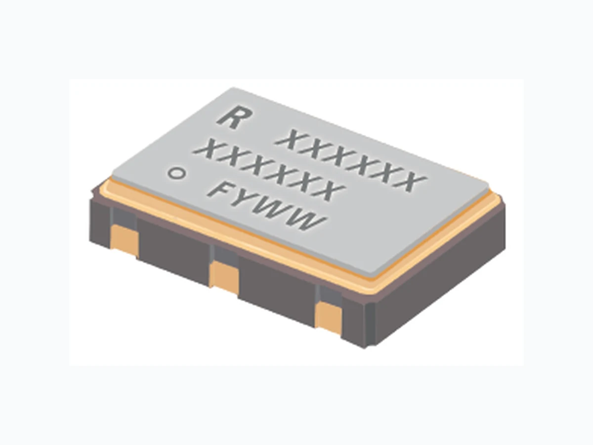
9.0 SSB PHASE NOISE Line Parameter Test Condition Value Unit 9.1 SSB Phase Noise power density @ 10 Hz offset Typical value for a 122.88 MHz VCXO @ 25 °C -67 dBc/Hz 9.2 SSB Phase Noise power density @ 100 Hz offset Typical value for a 122.88 MHz VCXO @ 25 °C -98 dBc/Hz 9.3 SSB Phase Noise power density @ 1 kHz offset Typical value for a 122.88 MHz VCXO @ 25 °C -127 dBc/Hz 9.4 SSB Phase Noise power density @ 10 kHz offset Typical value for a 122.88 MHz VCXO @ 25 °C -147 dBc/Hz 9.5 SSB Phase Noise power density @ 100 kHz offset Typical value for a 122.88 MHz VCXO @ 25 °C -150 dBc/Hz ----- 10.0 PIN CONNECTIONS Line Parameter 10.1 Pin 1 VCO 10.2 Pin 2 E/D* or NC 10.3 Pin 3 GND 10.4 Pin 4 OUTPUT 10.5 Pin 5 COMPLIMENTARY OUTPUT (LVPECL/LVDS only) or NC 10.6 Pin 6 VDD 10.7 * Output Enabled >70% of VDD on E/D pin, or E/D pin left open (connected to internal pull-up resistor) 10.8 * Output Disabled <30% of VDD on E/D pin, or E/D pin to GND ----- 11.0 PACKAGE DETAIL Line Parameter 11.1 Package F 11.2 Top Line 11.3 Middle Line 11.4 Bottom Line [o FYWW] Pin 1, Manufacturing code, Year code* and Week code** 11.5 * Year Code A = 2010, B = 2011, C = 2012, D = 2013, ... Z = 2035 11.6 ** Week Code WW = 01 = Week of first Monday of the year ----- 12.0 ENVIRONMENTAL SPECIFICATION Line Parameter 12.1 Mechanical Shock MIL-STD-883, Method 2002 12.2 Storage Temperature Range -55 to 125°C 12.3 Humidity After 48 hours at 85°C±2°C 85% humidity non-condensing 12.4 Thermal Shock MIL-STD-883, Method 1011 12.5 Vibration MIL-STD-883, Method 2007 12.6 Gross and Fine Leak MIL-STD-883, Method 1014 12.7 RoHS Compliant Yes ----- 13.0 MANUFACTURING INFORMATION Line Parameter 13.1 Packaging Description Tape and reel. Standard packing quantity is 4000 per reel 13.2 Reflow Solder reflow process as per attached profile Page 3
Drawing Name: XO/VCXO 5032 6-Pin Model Drawing Page 4
Drawing Name: XO/VCXO 6 Pin Series Test Circuit Page 5
Drawing Name: XO/VCXO5032 F Series Tape & Reel Page 6
Drawing Name: Pb-Free Reflow Page 7