
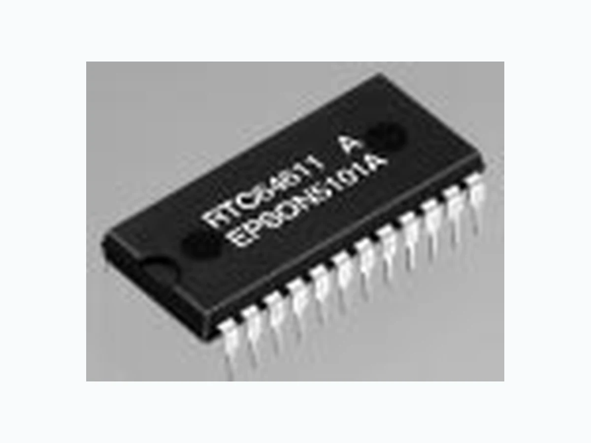
RTC-64611 ETC1
Document overview
- Manufacturer or author: Provided By www.digicamel.com(FREE DATASHEET DOWNLOAD SITE)
- PDF pages: 2
Technical content
Specifications (characteristics) Absolute Max. rating Operating range Frequency characteristics and current consumption characteristics DC characteristics External dimensions Terminal connection (Unit: mm ) RTC-64611 RTC64613 A EPSON 9360A RTC 64611 A EPSON 5101A (VDD) is to be same level as VDD. Do not connect it to any external terminals. NC is not connected internally. RTC-64613 32.0 max. 13.6 4.43.3 0.8 15.24 0.25 2.5 16.3 max. 7.9 12.2 max. 1.0 0.3 0.2 Unless otherwise stated, characteristics (specifications) shown in the above table are based on the rated operating temperature and voltage condition. (VDD = 5V – 0.5V, Ta = -20 to + 75˚C) No. No. GND H-START/STOP IRQ 1HZ I/O 1 I/O 2 I/O 3 GND Pin terminal I/O 4 I/O 5 I/O 6 I/O 7 I/O 8 CS OE WE NC DD) (VDD) VDD Pin terminal 0° to 10° 90° to 105° 0.05 min. 2.8 max. 8-bit REAL TIME CLOCK MODULE RTC-64611/64613
- Builtin crystal unit allows adjustment-free efficient operation.
- 8-bit data bus and high speed access (85 nsec. max.).
- Provided with the same interface as S-RAM and battery backup function.
- Interruption of alarm of sec. to day and day of week and carry interruption.
- Reference signal selectable in a range of 1 Hz to 64 Hz (binary).
- Leap year automatically adjustable (gregorian calendar).
- With 1 Hz output terminal.
- Provided with START/STOP, 30 second adjust function.
- RTC-64613 uses a similar mounting method to that of a normal SMD IC. Item Power source voltage Input voltage Storage temperature Soldering condition Symbol VDD VIN TSTG TSOL Condition Ta=25˚C RTC-64611 RTC-64613 RTC-64611 RTC-64613 Specifications -0.5 to 7.0 -0.5 to VDD+0.3 -55 to +85 -55 to +125 Under 260˚C within 10 sec. (lead part) (package should be less than 150˚C) Twice at under 260˚C within 10 sec. or under 230˚C within 3 min. Unit V Item Operating voltage Operating temperature Data holding voltage CS data holding time Operation restoring time Symbol VDD TOPR VDH tCDR tR Condition CS ‡VDD - 0.2V Specifications 4.5 to 5.5 -20 to + 75 2.0 to 4.5 0 min. tRC (85 ns.) Unit V V ns Item Frequency tolerance Frequency temperature characteristics Aging Shock resistance Current consumption Symbol Df/fo fa S.R. IDD 1 IDD 2 Ta=25˚C VDD=5V 64611 A 64611 B 64613 A 64613 Condition Three drops on a hard board from 75 cm or 3000G x 0.3ms x 1/2 sine wave x 3 directions No load__ CS ‡ 1.8V VDD=5V VDD=2V Specifications +15/-5(5±10) +55/-45(5±50) +25/-15(5±20) +55/-45(5±50) +10/-120 +10/-220 ±5 max. ±10 max. 2 max. Unit ppm ppm/Y ppm mA µA -10 to +70˚C(25˚C reference temperature) -20 to +75˚C(25˚C reference temperature) VDD=5V, Ta=25˚C, first year Item “H” input voltage “L” input voltage Input leak current Three-state leak current Output leak current (except for 1 Hz, IRQ) “L” output voltage Input capacity Output capacity Symbol VIH VIL IIN ITSL ILOH VOH VOL CIN COUT Condition IOH=-1mA IOL=2.1mA VIN=OV Ta=25˚C f =1.0 MHz Min. 2.2 -0.3 2.4 Max. VDD 0.8 ± 2 ±10 0.4 12.5 Unit V µA V pF Min. VDD -0.2 -0.3 Max. VDD 0.2 ± 2 ±10 VDD= 5V±10% VDD= 2V Actual size
32.768 KHZ
Switching characteristic Register table Block diagram Supplement
16 KHz
2 KHz
8 KHz
1 KHz
4 KHz
64 Hz register / counter
64 Hz alarm. register Alarm comparison circuit Sec. alarm. register Min. alarm. register Hour alarm. register Day-of-week alarm. register Day alarm. register Control register A Control register B Sec. register / counter Min. register / counter Hour register / counter Day-of-week register / counter Day register / counter Month register / counter Year register / counter
1 Hz 1 Hz
H • START / STOP Write Read Data bus Bus interface circuit I/0 1 to I/03 Address bus A 0 to A3 CS OE WE IRQ Address OE CS D OUT Data valid tRC tAA tACS tOH tOHZ tOHZ tCHZ tOE tOLZ tOH VOL VOL VOL VOL OE CS D OUT D IN Address tWC tCW tAW tW-R tAS tOHZ WE tWP tDW tDH Measuring condition Input pulse level: 0.8 to 2.4V Input rise time, fall time: 5 nsec. IN/OUT timing pulse level: 1.5V Out put load: 1 TTL Gate +100pF Note: Do not enter erroneous data for clock. This may result in time keeping error. Be sure to enter “O” to TEST bit.∗1 A B C D E F b Address Data 1 Hz 2 Hz 4 Hz 8 Hz 16 Hz 32 Hz 64 Hz 10-sec. digit 10-min. digit 1-sec. digit 1-min. digit 1-hour digit10-hour digit* * * 10-day digit 10-month digit 10-year digit
1 Hz 2 Hz 4 Hz 8 Hz 16 Hz 32 Hz 64 Hz
*1 30-sec. adjustment RESET S.START /STOP Alarm flag Carry interruption enable Alarm interruption enable 10-sec. digit 10-min. digit 10-hour digit 10-day digit Day-of-week digit 1-day digit 1-month digit 1-year digit 1-sec. digit 1-min. digit 1-hour digit Day-of-week digit 1-day digit Remarks Counter Alarm register Control register Bit name * mark 10-hour digit (b5) Under-sec. counter Under-sec. alarm register Sec.to year Day of week
Description
Recognized as “0” while reading Only for 24H mode Read only (unwriteable) Used as binary code data Used as binary code data Both counter and alarm register use BCD code Coded data is used EX: 0…Sunday 1…Monday 2…Tuesday 3…Wednesday 4…Thursday 5…Friday 6…Saturday Item Read cycle time Address access time Chip select access time Output enable access time Output hold time Chip select / output set time Output enable / output set time Chip deselect / output floating Output disable / output floating Symbol t RC tAA tACS tOE tOH tCLZ tOLZ tCHZ tOHZ Min. Max. Unit ns Item Write cycle time Chip select time Address valid time Address setup time Write pulse time Address holding time ___ WE output floating Input data set time Input data hold time Output disable / output floating ___ WE output set time Symbol t WC tCW tAW tAS tWP tWR tWHZ tDW tDH tOHZ tOW Min. Max. Unit ns