
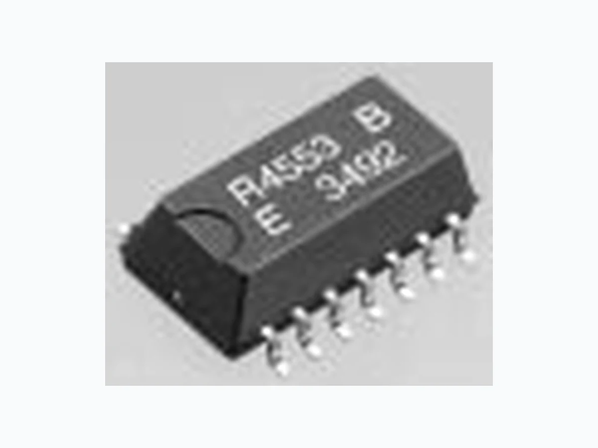
RTC4553 ETC
Document overview
- Manufacturer or author: Provided By www.digicamel.com(FREE DATASHEET DOWNLOAD SITE)
- PDF pages: 2
Technical content
Absolute Max. rating Specifications (characteristics) Operating range Frequency characteristics DC characteristics External dimensions (Unit: mm) R4553 A 6496E 7.4–0.23.2–0.1 5.03.1 10.1–0.2 Terminal connection 0.150.6 0.05 min. No. Pin terminal GND WR SIN SCK No. Pin terminal TPOUT SOUT CS1 CS0 V DD 1234567 14 13 12 11 10 9 8 VDD=5V–10% (GND=OV, Ta=-30˚C to +70˚C) VDD=3V–10% (GND=OV, Ta=-30˚C to +70˚C) L1 to L5 are test pin. Do not connect them to any terminals. SERIAL-INTERFACE REAL TIME CLOCK MODULE RTC-4553 Item Supply voltage Input voltage Output voltage Storage temperature Soldering conditions Symbol V DD VIN VOUT TSTG TSOL Condition VDD-GND SIN,SCK , W R, CS 0, CS1 SOUT, TPOUT ____ Stored without tape & reel Min. -0.3 -55 Max. +6.0 VDD+0.3 +125 Unit V Twice at under 260˚C within 10 sec. or under 230˚C within 3 min. Item Operating voltage Operating temperature Symbol VDD TOPR Condition Min. 2.7 -30 Typ. 5.0 Max. 5.5 +70 Unit V Item Frequency tolerance Frequency temperature characteristics Frequency voltage characteristics Aging Symbol Df/fo Top fv fa Condition Ta=25˚C, VDD=5V AA A B Ta=-10 to 70˚C, VDD=5V Reference at 25˚C Ta=Fix, VDD=2 to 5.5V Reference at 5V Ta=25˚C, VDD=5V, first year Range 5±5 5±10 5±20 +10 -120 Unit ppm ppm/ year Item Data holding voltage Current consumption Output voltage Off leak current Input voltage Input current Oscillation start-up time Item Data holding voltage Current consumption Output voltage Off leak current Input voltage Input current Oscillation start-up time Symbol VDH IDD1 IDD2 VOH VOL IOZH IOZL VIH VIL IIH IIL Tosc Condition SCK ___ =500 kHz SCK ___ =DC IOH=-400µA IOL=1.6mA VOUT=5.5V VOUT=0V VIN=5.5V VIN=0V Ta=25˚C Min. 2.0 VDD-0. 4 -2.0 4/5 VDD -2.0 Typ. 1.0 Max. 5.5 100 3.0 0.4 2.0 1/5 VDD 2.0 3.0 Unit V µA V µA V µA s Unit V µA V µA V µA s Symbol VDH IDD1 IDD2 VOH VOL IOZH IOZL VIH VIL IIH IIL Tosc Condition SCK ___ =300 kHz SCK ___ =DC IOH=-400µA IOL=1.6mA VOUT=3.3V VOUT=0V VIN=3.3V VIN=0V Ta=25˚C Min. 2.0 VDD-0.4 -2.0 4/5 VDD -2.0 Typ. 1.0 Max. 3.3 100 3.0 0.4 2.0 1/5 VDD 2.0 3.0
- Builtin crystal unit allows adjustment-free efficient operation.
- The small package makes high-density mounting possible. (SOP 14-pin)
- Automatic calendar function (year, month, day, day of the week, hour, minute, second).
- Automatic leap year correction. (up to 2099)
- Builtin 30 x 4-bit S-RAM.
- High-speed access.
- Reference pulse output. (1024 Hz, 1/10 Hz)
- Low current consumption. (1 µA typical)
- Similar mounting method to that used for universal type SMD IC. Actual size
32.768 kHz TP OUT SOUT SCK SIN CS 1 CS 0 WR (Ta=-30˚C to +70˚C, VDD=5V–10%, GND=OV) Note: ∗ TEST bit should be “0”. CS0 SCK SIN WR SOUT SOUT CS1 TPOUT SCK CS0 t WCKL t SD t SWR t DSZ1 t DSO t DPZ1 t DPZ2 t DSZ2 t PS t HWR t HD t WCKH t HCS 1/f CLK 10% 90% 90% 90% 10% 10% 90% 90% 90% 90% 10% 10% 10% 10% 90% 10% 10% tSCS SCK OSC Counter Output control RAM (120bit) Input control Output control Shift register Control circuit Control register Control register Control register Sec. Min. Hou. Day of Week Day Mon. Year Address A B C D E F A A A A MODE 0 Counter control registerRegister symbol S S10 MI1 MI10 H10 W D10 MO1 MO10 Y10 mi8 PM/AM mo8 y80 TPS BUSY SYSR D S40 mi4 mi40 mo4 y40 30ADJ PONC TEST S20 mi2 mi20 h20 d20 mo2 y20 CNTR MS1 S10 mi1 mi10 h10 d10 mo1 mo10 y10 MS0 Register name 1-second digit register 10-second digit register 1-minute digit register 10-minute digit register 1-hour digit register 10-hour digit register Day of the week digit register 1-day digit register 10-day digit register 1-month digit register 10-month digit register 1-year digit register 10-year digit register Control register 1 Control register 2 Control register 3 MODE 1 User RAM Domain 1 D RA3 RA7 RA11 RA15 RA19 RA23 RA27 RA31 RA35 RA39 RA43 RA47 RA51 RA55 RA59 RA2 RA6 RA10 RA14 RA18 RA22 RA26 RA30 RA34 RA38 RA42 RA46 RA50 RA54 RA58 RA1 RA5 RA9 RA13 RA17 RA21 RA25 RA29 RA33 RA37 RA41 RA45 RA49 RA53 RA57 RA0 RA4 RA8 RA12 RA16 RA20 RA24 RA28 RA32 RA36 RA40 RA44 RA48 RA52 RA56 MODE 2 User RAM Domain 2 RA63 RA67 RA71 RA75 RA79 RA83 RA87 RA91 RA95 RA99 RA103 RA107 RA111 RA115 RA119 RA62 RA66 RA70 RA74 RA78 RA82 RA86 RA90 RA94 RA98 RA102 RA106 RA110 RA114 RA118 RA61 RA65 RA69 RA73 RA77 RA81 RA85 RA89 RA93 RA97 RA101 RA105 RA109 RA113 RA117 RA60 RA64 RA68 RA72 RA76 RA80 RA84 RA88 RA92 RA96 RA100 RA104 RA108 RA112 RA116 Same as MODE 0 Same as MODE 0 Item SCK ___ input frequency SCK ___ “L” time SCK ___ “H” time SCK ___ pause time CS0 setup time CS0 hold time SIN data setup time SIN data Hold time WR ___ setup time WR ___ hold time SOUT delay time CS0 , and CS1 enable to SOUT output CS0 disenable to SOUT high Z CS1 enable to SOUT output CS1 enable to SOUT high Z Symbol fSCK tWSCKL tWSCKH tPS tSCS tHCS tSD tHD tSWR tHWR tDSO tDSZ1 tDSZ2 tDPZ1 tDPZ2 Condition CL=100pF Min. 1.0 0.5 0.2 1.0 0.5 Typ. 150 Max. 500 500 100 Unit kHz µs ns