
DATASHEET SEARCH SITE
Document overview
- Manufacturer or author: Provided By www.digicamel.com(FREE DATASHEET DOWNLOAD SITE)
- PDF pages: 2
Technical content
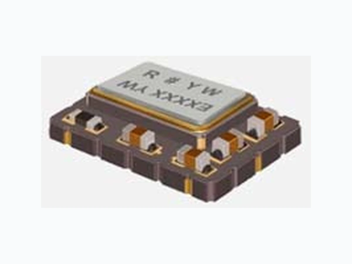
PLUTO+ ™ ULTRA STABLE SMD TCXO www.rakon.com sales@rakon.com Page 1 of 2 RPT7050A The RPT7050A encompasses Rakon's new patented Pluto+ ASIC. Pluto+ advances on the world famous, ‘best‐in‐class’Pluto ASIC technology by delivering exceptional phase noise and jitter performance and enhanced frequency versus temperature stability. The single chip oscillator with its analogue compensation circuit is capable of sub 0.1ppm frequency stability over an extended temperature range and RMS phase jitter down to 0.13ps for IEEE1588 and SyncE applications. Its patented, unique tilt control ensures lifetime specification compliance, unlike other TCXOs available. Standard Specifications Parameter Min. Typ. Max. Unit Test Condition / Description Nominal frequency 1.25 – MHz Standard frequencies: 10.0, 12.8, 16.384, 19.2, Frequency calibration ±1 ppm Initial accuracy at 25 ± 1°C Reflow shift ±0.5 ppm Pre to post reflow ΔF (measured ≥ 60 minutes after reflow) Operating temperature range ‐ 55 105 °C Frequency stability over temperature ±0.05 – ±2.5 ppm Reference to (Fmax + Fmin)/2. The best available stability depends on the nominal frequency and selected operating temperature range Supply voltage stability ±0.025 ppm ±5% variation Reference to frequency at nominal VCC Load sensitivity ±0.05 ppm HCMOS, ACMOS: ±5pF variation, Clipped sine wave / Sine wave: ±10% variation reference to frequency at nominal load Long term stability (aging) ≤26MHz >26MHz ppm/year ppm/year ±3ppm/10 years ±5ppm/10 years Acceleration stability <2 ppb/g Gamma vector, 3 axes, 30 – 1500Hz Start‐up time 5 – 15 ms 90% amplitude Supply voltage, VCC Current (C/Sine) Current (Sine) Current (HCMOS) Current (ACMOS) 2.5 5.7 V mA mA mA mA ±5%, standard values are 3.0, 3.3 and 5.0V Control voltage, Vc 0.5 2.5 V Frequency tuning ≤26MHz >26MHz ppm ppm Root Allan Variance (20MHz) 5 10‐11 tau = 1.0s Oscillator output options Clipped sine wave, sine wave, HCMOS (LVCMOS & LVTTL compatible as per JESD8C) and ACMOS Tri‐state control Input level low (pin 6) Input level high (pin 6) 0.6VCC 0.2VCC V V Device disabled, output in high impedance state Device enabled and operating Features Applications 7.0 x 5.0 x 2.0 mm Best in class frequency versus temperature RMS phase jitter down to 0.13ps Phase noise <‐160dBc/Hz noise floor Voltage control and T‐sense options available Time and frequency reference o Positioning o Test and Measurement o Telecommunications o Hi‐Rel / Defense
PLUTO+ ™ ULTRA STABLE SMD TCXO www.rakon.com sales@rakon.com Page 2 of 2 SSB Phase Noise (Typical value at 25°C) Model Outline and Recommended Pad Layout Test Circuit RMS Jitter = 140 fs (12 kHz ~ 5 MHz) RMS Jitter = 300 fs (12 kHz ~ 5 MHz)